Liquid crystal display device and color filter substrate

a display device and color filter substrate technology, applied in the field of liquid crystal display devices, can solve the problems of increasing the thickness and weight of portable equipment, and not disclosing a detection accuracy enhancement techniqu

Active Publication Date: 2015-11-26
TOPPAN PRINTING CO LTD
View PDF5 Cites 19 Cited by
  • Summary
  • Abstract
  • Description
  • Claims
  • Application Information

AI Technical Summary

Problems solved by technology

In a case where an on-cell type touch panel is provided in portable equipment or the like, thickness and weight of the portable equipment increases.
However, the patent literatures 1 and 2 do not disclose a position detecting technique in which a transparent electrode pattern of X-direction and a transparent electrode pattern in the Y-direction are formed on a transparent substrate such as a glass substrate and high-precision touch sensing by a pointer is accomplished.
However, patent literature 3 does not disclose a technique that enhances detection accuracy of electro capacitive type touch sensing.
However, patent literature 4 does not disclose a technique that enhances detection accuracy of electro capacitive type touch sensing.
In a case where a protrusion of the colored layer which is formed when the colored layer is coated on the black matrix having a thickness of 2 μm and a variation of a film thickness of the colored pixels become large, liquid crystal alignment fluctuates so that it is hard to perform liquid crystal display in an uniform manner.

Method used


Image

  • Liquid crystal display device and color filter substrate
  • Liquid crystal display device and color filter substrate
  • Liquid crystal display device and color filter substrate

Examples


first embodiment

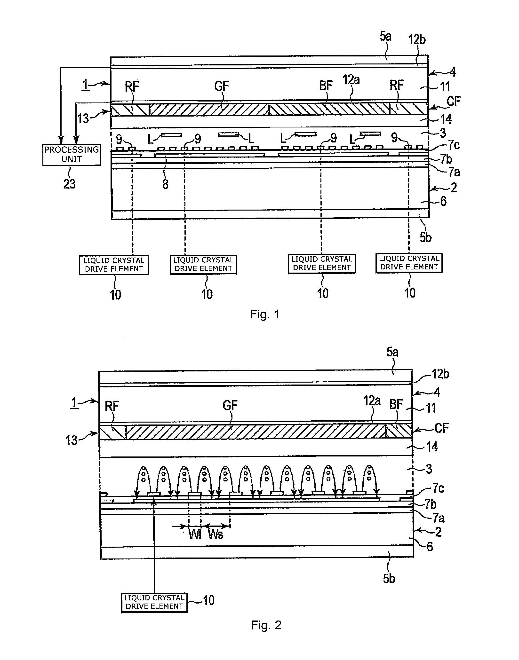
[0048]FIG.1 and FIG. 2 are cross sectional view showing an example of a liquid crystal display 1 provided in the liquid crystal display device according to the present embodiment. FIG.1 exemplifies a cross section along the horizontal direction of a red pixel RP, a green pixel GP and a blue pixel BP. FIG. 2 exemplifies a cross section along the horizontal direction of the green pixel GP.

[0049]In FIG. 1 and FIG. 2, an upper side of the liquid crystal panel 1 (hereinafter may be referred to as a front side or display surface side) is an observer side and an lower side of the liquid crystal panel 1 (back side) is an internal side of the liquid crystal display device. The liquid crystal display device is provided with, in the lower side of the liquid crystal panel 1, an optical control element which is not shown and a backlight unit which is not shown.

[0050]The liquid crystal panel 1 is provided with an array substrate 2, liquid crystal layer 3 and a color filter substrate 4. The array ...

second embodiment

[0116]According to the present embodiment, modifications of the above-described first embodiment will be described.

[0117]FIG. 15 is a cross sectional view showing an example of the color filter substrate 19 according to the present embodiment. The color filter substrate 19 has a configuration in which transparent substrate electrode layers 12a and 12b are respectively formed on both surfaces of the transparent substrate 11 and a color filter layer 13, a transparent resin layer 14, a light shielding layer 20 and a transparent resin layer 21 are laminated on the transparent electrode layer 12a. FIG. 15 is illustrated under a condition that the above-described FIG. 11 and the film surface (surface of the color filter CF) are positioned to be opposite from each other, i.e., the transparent electrode layer 12b is positioned to be on the lower side and the transparent resin layer 21 is positioned to be on the upper side.

[0118]The major difference between the color filter substrate 4 accor...

third embodiment

[0145]In the present embodiment, hereinafter will be described modifications of the first and second embodiments described above. According to the present embodiment, modifications of the color filter 4 are described. Similarly, modifications can be applied to the color filter 19. Further, in the present embodiment, a manufacturing method of the color filter substrate is described as well.

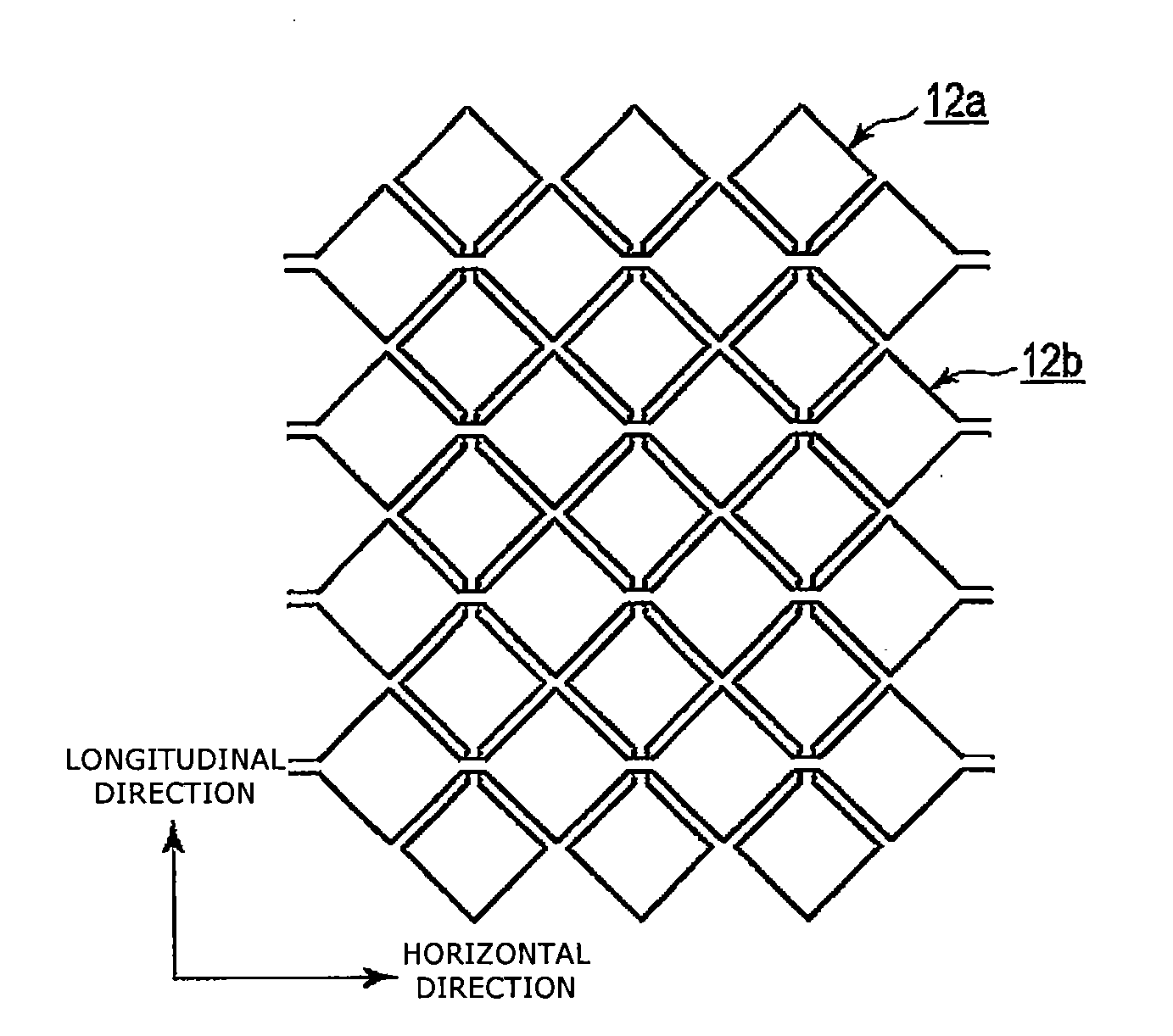
[0146]According to the present embodiment, a plurality of pixels may include a pixel of which width in the horizontal direction (hereinafter referred to as horizontal width) is ½ that of other pixels. The pixel having ½ horizontal width has its long side in the longitudinal direction. However, the plurality of pixels may include, as an alternative to a pixel having an elongated shape in the longitudinal direction, pixels of which width in the longitudinal direction (hereinafter referred to as longitudinal width) is ½ that of other pixels. In this case, the pixels having ½ longitudinal width have a ...


PUM


Abstract

A liquid crystal display device having a touch panel function includes an array substrate, a liquid crystal layer including a liquid crystal molecule, and a color filter substrate positioned over the array substrate via the liquid crystal layer. The color filter substrate includes a transparent substrate, first and second transparent electrode layers, a color filter formed on the first transparent electrode layer and including a red filter, a green filter and a blue filter, and a transparent resin layer formed on the color filter. The color filter and the transparent resin layer have a total thickness in a range of approximately from 2.5 μm to 9 μm. The liquid crystal molecule has negative dielectric anisotropy and an initial state alignment which is parallel to a substrate surface. The liquid crystal molecule rotates within a plane parallel to the substrate surface when a liquid crystal drive voltage is applied.

Description

CROSS-REFERENCE TO RELATED APPLICATIONS[0001]The present application is a continuation of International Application No. PCT / JP2013 / 057556, filed Mar. 15, 2013, which is based upon and claims the benefits of priority to Japanese Application No. 2013-017599, filed Jan. 31, 2013. The entire contents of these applications are incorporated herein by reference.BACKGROUND OF THE INVENTION[0002]1. Field of the Invention[0003]The present invention relates to a liquid crystal display device having a touch sensing function and a color filter used for the same.[0004]2. Discussion of the Background[0005]In a touch sensing operation in which a location of a pointer or an operation is detected, on-cell type touch panels have been widely used for liquid crystal display devices. On-cell type touch panels are provided on each liquid crystal cells. Types of touch panel include an electrostatic capacitance type, resistive film type, optical type, electromagnetic induction type or the like. In recent ye...

Claims


Application Information

Patent Timeline
Patent Type & Authority Applications(United States)
IPC IPC(8): G02F1/1335G02B5/22G02F1/137G02B5/20G02F1/1333G02F1/1343
CPCG02F1/133514G02F1/13338G02F1/13439G02F1/134309G02F2001/13712G02B5/201G02F1/133512G02B5/223G02F1/137G06F3/0412G06F2203/04103G06F3/0445G06F3/0446G02F1/13712
Inventor KIMURA, YUKIHIROFUKUYOSHI, KENZO
Owner TOPPAN PRINTING CO LTD
Why Eureka
Try Eureka