An array substrate and display device

a display device and substrate technology, applied in the field of display, can solve the problem of low aperture ratio of the existing liquid crystal display device, and achieve the effect of low aperture ratio

Active Publication Date: 2015-12-17
SHENZHEN CHINA STAR OPTOELECTRONICS TECH CO LTD
View PDF4 Cites 9 Cited by
  • Summary
  • Abstract
  • Description
  • Claims
  • Application Information

AI Technical Summary

Benefits of technology

[0006]The purpose of the present disclosure is to provide an array substrate and display device so as to solve the technical problem of low aperture ratio in the existing liquid crystal display device.

Problems solved by technology

Therefore, there exists the technical problem of low aperture ratio in the existing liquid crystal display device.

Method used


Image

  • An array substrate and display device
  • An array substrate and display device
  • An array substrate and display device

Examples


embodiment 1

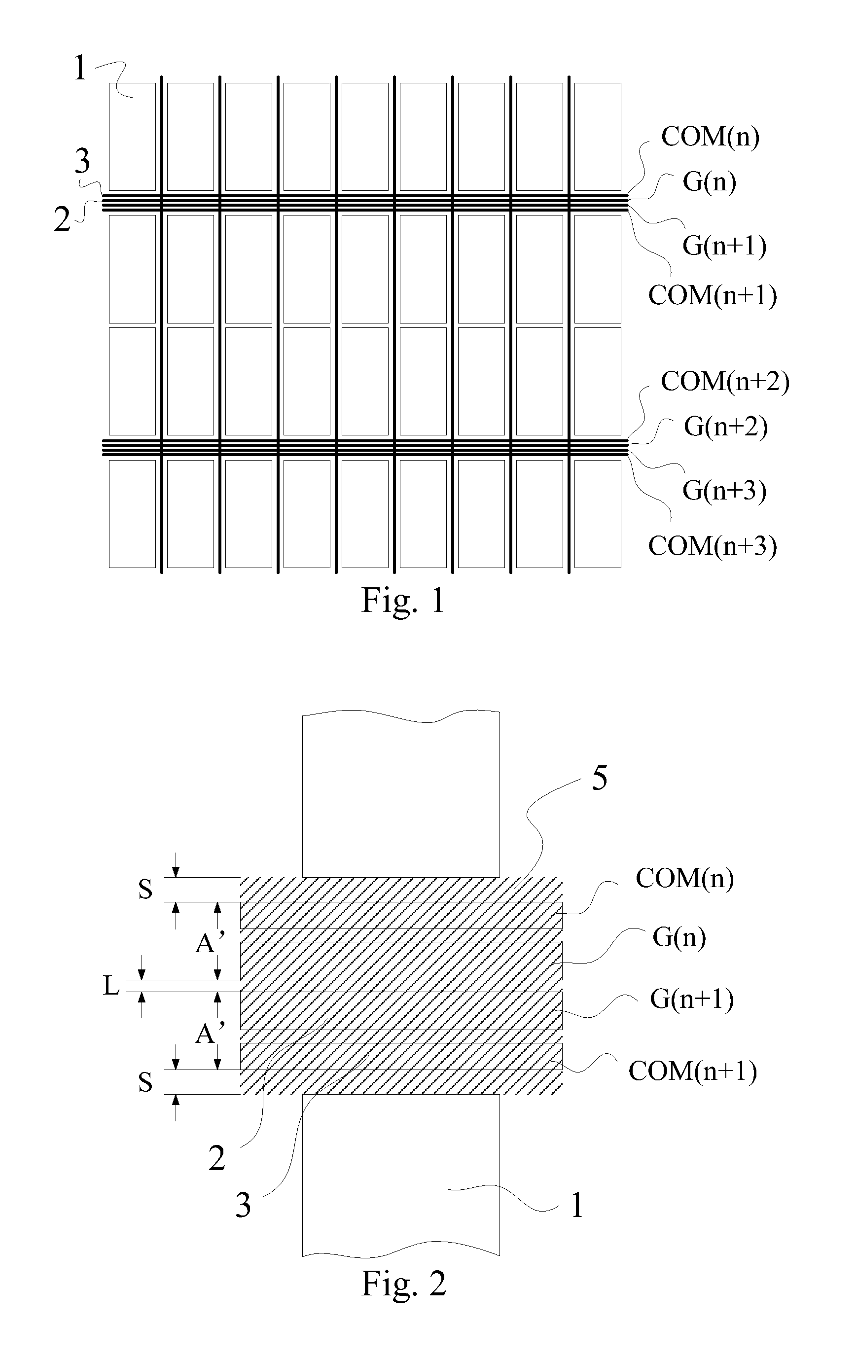
[0036]The array substrate in embodiment 1 of the present disclosure comprises a plurality of sub pixel units arranged in an array and a plurality of signal lines. The signal lines of the present embodiment are gate lines 2 corresponding to sub pixel units 1 in each row, as shown in FIG. 1. With respect to two adjacent gate lines 2, for example G(n) and G(n+1), G(n) is arranged below (a first side) its corresponding sub pixel units 1, and G(n+1) is arranged above (a second side) its corresponding sub pixel units 1 (said first side and said second side being one of opposite sides of two rows of the sub pixel units respectively). For another example, in two adjacent gate lines G(n+2) and G(n+3), G(n+2) is arranged below its corresponding sub pixel units 1, and G(n+3) is arranged above its corresponding sub pixel units 1.

[0037]In addition, G(n+1) and G(n+2) can also be seen as two adjacent gate lines, in such case, G(n+2) is arranged below (the first side) its corresponding sub pixel un...

embodiment 2

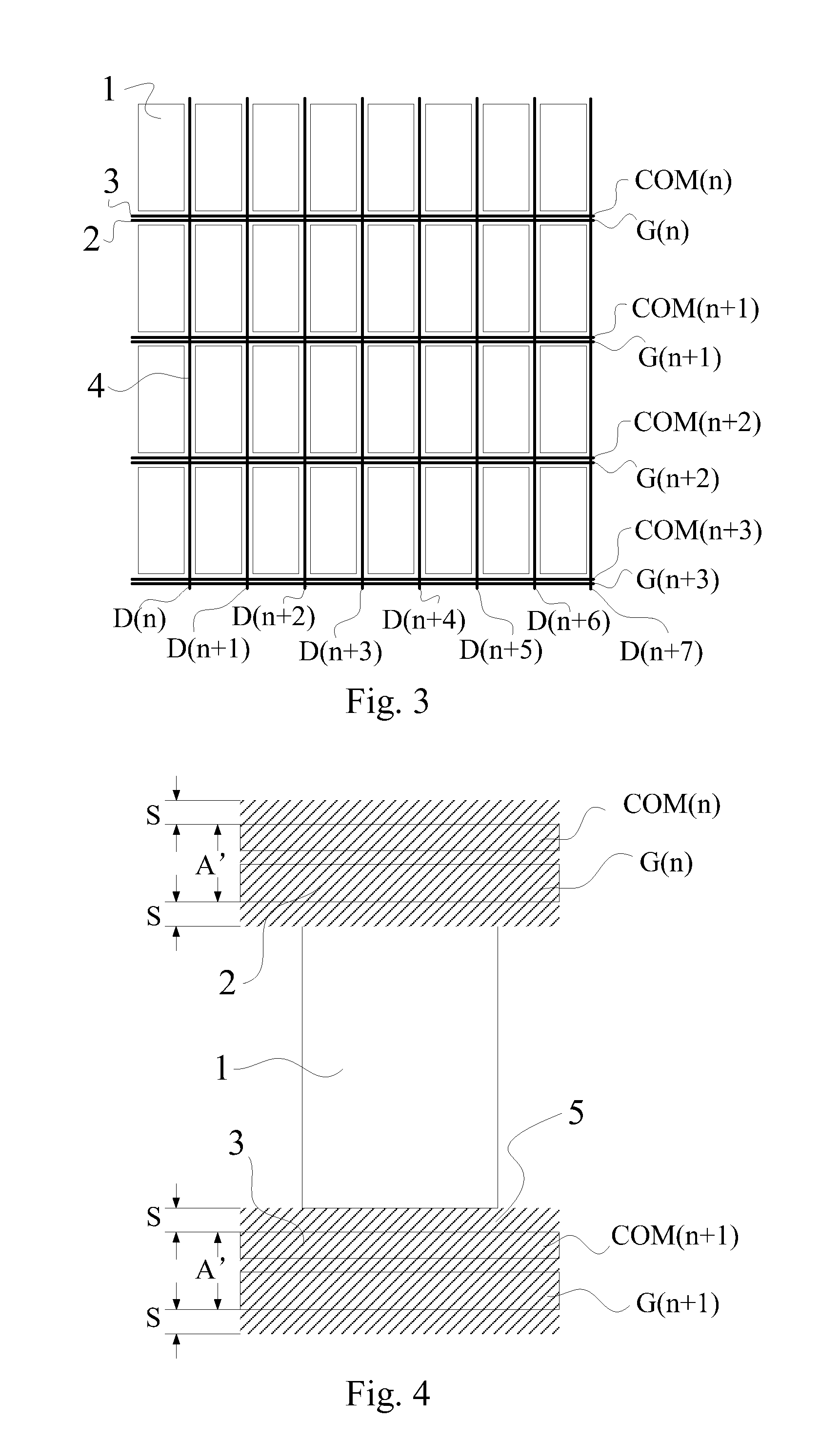
[0045]The present embodiment is substantially same as embodiment 1. The array substrate comprises a plurality of sub pixel units 1 arranged in an array and a plurality of gate lines, as shown in FIG. 5. With respect to two adjacent gate lines 2, for example G(n) and G(n+1), G(n) is arranged below its corresponding sub pixel units 1, and G(n+1) is arranged above its corresponding sub pixel units 1. For another example, with respect to two adjacent gate lines G(n+2) and G(n+3), G(n+2) is arranged below its corresponding sub pixel units 1, and G(n+3) is arranged above its corresponding sub pixel units 1.

[0046]The differences of present embodiment from embodiment 1 lie in that: as shown in FIG. 5, each of said sub pixel units 1 comprises a storage capacitor 6 and a pixel electrode (not shown in FIG. 5), wherein one end of said storage capacitor 6 is connected with the gate line 2, and the other end of said storage capacitor 6 is connected with said pixel electrode. Particularly, part of...

embodiment 3

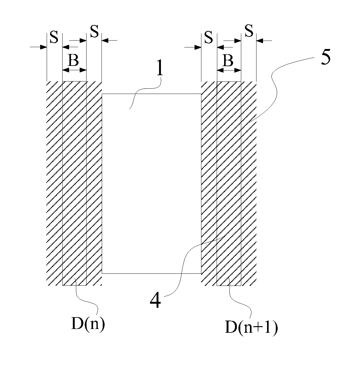
[0048]The array substrate provided by embodiment 3 of the present disclosure comprises a plurality of sub pixel units 1 arranged in an array and a plurality of signal lines. The signal lines in the present embodiment are data lines 4 corresponding to the sub pixel units 1 in each column, as shown in FIG. 7. With respect to two adjacent data lines 4, for example D(n) and D(n+1), D(n) is arranged in the right side (a first side) of corresponding sub pixel units 1, and D(n+1) is arranged in the left side (a second side) of corresponding sub pixel units 1 (said first side and said second side being one of opposite sides of the sub pixel units respectively). For another example, in two adjacent data lines D(n+2) and D(n+3), D(n+2) is arranged in the right side of corresponding sub pixel units 1, and D(n+3) is arranged in the left side of corresponding sub pixel units 1.

[0049]In addition, D(n+1) and D(n+2) can be seen as two adjacent data lines, in such case, D(n+2) is arranged in the rig...


PUM

PropertyMeasurementUnit
areaaaaaaaaaaa
coloraaaaaaaaaa
widthaaaaaaaaaa

Abstract

The present disclosure discloses an array substrate, belongs to the technical field of display technology, and solves the technical problem of low aperture ratio of prior liquid crystal display device. The array substrate comprises a plurality of sub pixel units arranged in an array and a plurality of signal lines, wherein one signal line of two adjacent signal lines is arranged in a first side of corresponding sub pixel units, and the other signal line is arranged in a second side of corresponding sub pixel units, said first side and said second side being one of opposite sides of the sub pixel units respectively. The array substrate of the present disclosure can be used in liquid crystal television, liquid crystal display, mobile phone, tablet personal computer and other display devices.

Description

CROSS REFERENCE TO RELATED APPLICATION[0001]The present application claims benefit of Chinese patent application CN 201410258802.2, entitled “An Array Substrate and Display Device” and filed on Jun. 11, 2014, which is incorporated herein by reference.FIELD OF THE INVENTION[0002]The present disclosure relates to the technical field of display, particularly, to an array substrate and display device.BACKGROUND OF THE INVENTION[0003]With the development of display technology, liquid crystal display has become the most commonly used flat panel display device.[0004]The liquid crystal display comprises an array substrate and a color film substrate. The array substrate is provided with a plurality of sub pixel units arranged in an array, and with gate lines and data lines arranged in a criss-cross pattern for separating each sub pixel unit. The array substrate is usually provided with common electrode lines parallel to the gate lines. The color film substrate is provided with a color film a...

Claims


Application Information

Patent Timeline
Patent Type & Authority Applications(United States)
IPC IPC(8): G02F1/1362G02F1/1343G02F1/1335H01L27/12
CPCG02F1/136286H01L27/124H01L27/1255G02F2001/134345G02F1/136213G02F1/133514G02F1/133512G02F1/134336G02F1/136209G02F2201/40
Inventor WANG, CONGSHIH, MING HUNGDU, PENG
Owner SHENZHEN CHINA STAR OPTOELECTRONICS TECH CO LTD
Why Eureka
Try Eureka