Solid-state image-sensing device

a solid-state image and image-sensing technology, applied in the scanning details of television systems, color television, television systems, etc., can solve the problems of increasing the size of each pixel, narrow dynamic range, and inability to acquire accurate information on subjects, etc., and achieve the effect of low aperture ratio

Inactive Publication Date: 2007-03-01
KONICA MINOLTA INC
View PDF5 Cites 18 Cited by
  • Summary
  • Abstract
  • Description
  • Claims
  • Application Information

AI Technical Summary

Benefits of technology

[0019] According to the present invention, the photoelectric charge that has overflowed from the photoelectric conversion element via the transfer gate is outputted as an overflow signal. Thus, according to the signal value of the overflow signal, it is possible to predict the integrated component to be added to the image signal. In this way, it is possible to realize a solid-state image-sensing device that has a pixel configuration similar to those conventionally adopted and that can be additionally furnished with an integrating capability easily. This helps prevent the solid-state image-sensing device from becoming unduly large or having an unduly low aperture ratio.

Problems solved by technology

This leads to a disadvantageously narrow dynamic range.
Thus, in situations where the amount of incident light is likely to vary, as during long-period exposure or in flash shooting, and in addition where a logarithmically converted image signal is outputted, as when the brightness of the subject is high, it is disadvantageously impossible to acquire accurate information on the subject.
This disadvantageously increases the size of each pixel, leading to a lower aperture ratio.

Method used


Image

  • Solid-state image-sensing device
  • Solid-state image-sensing device
  • Solid-state image-sensing device

Examples


Embodiment Construction

[0031] Hereinafter, embodiments of the present invention will be described below with reference to the drawings.

Configuration of an Image-Sensing Device

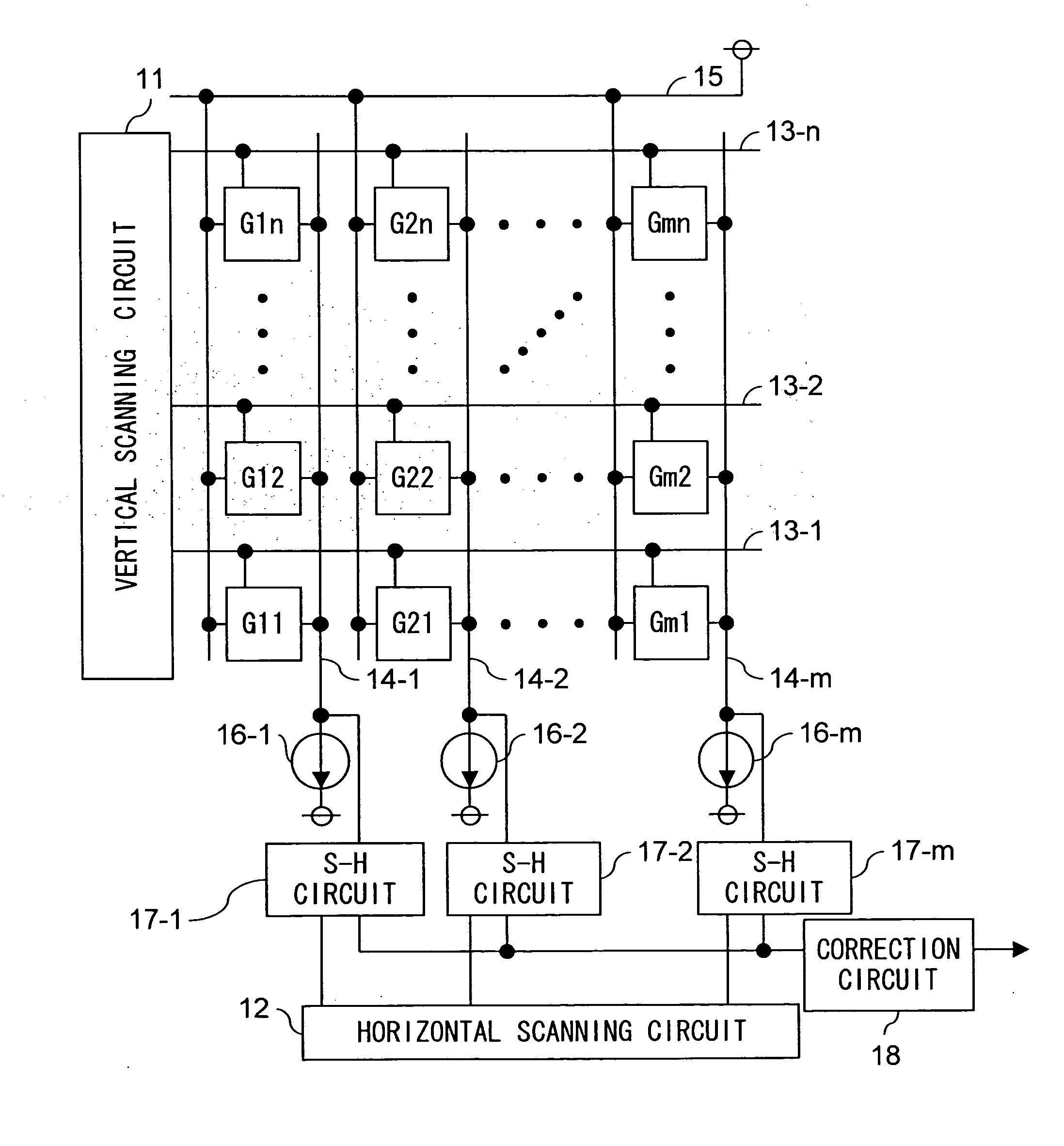
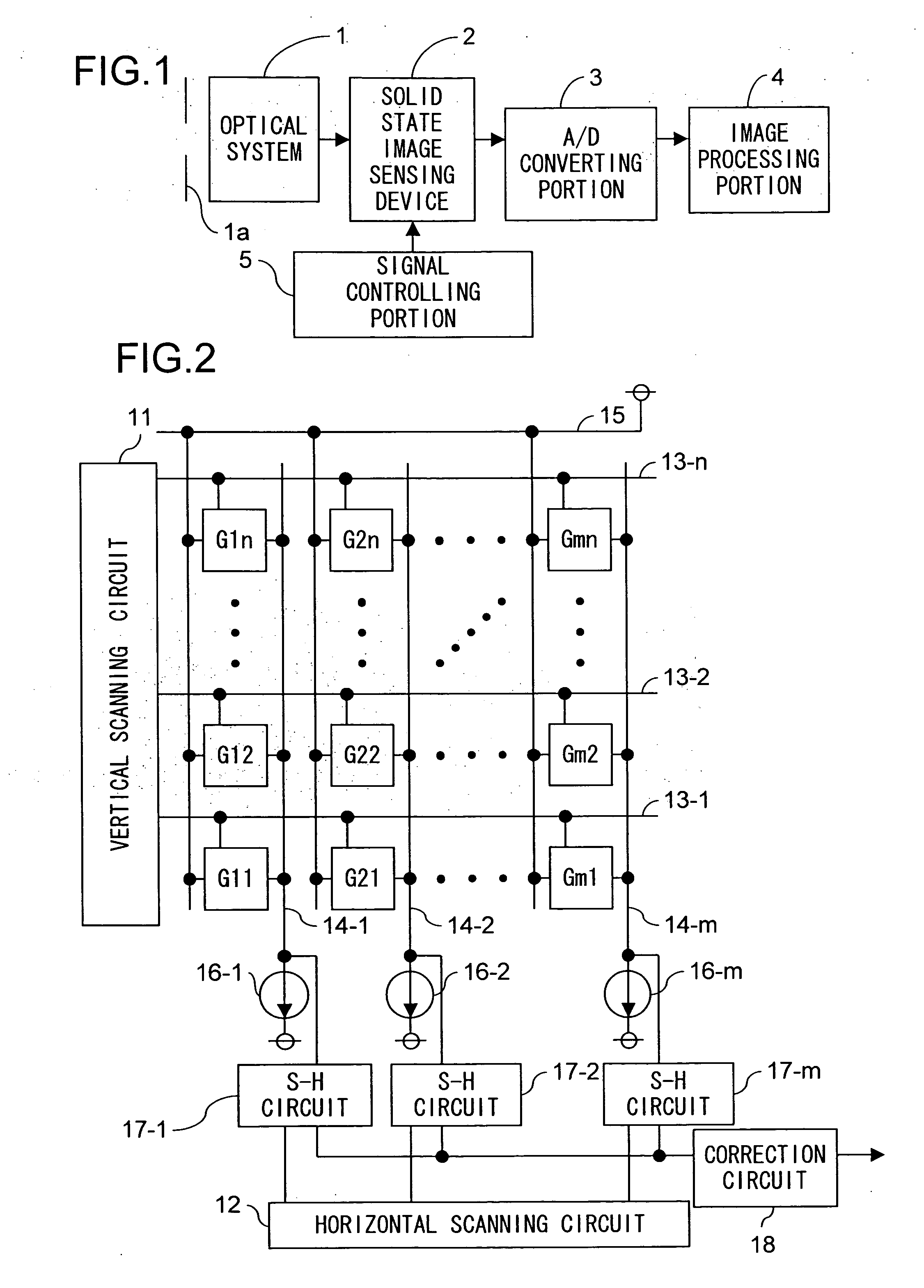
[0032] As shown in FIG. 1, an image-sensing device embodying the preset invention is provided with: an optical system 1 that is composed of a plurality of lenses; a mechanical shutter 1a that controls the exposure duration of the optical system 1; a solid-state image-sensing device 2 that converts the amount of light incident thereon through the optical system 1 into an electrical signal and outputs it as an image signal; an A / D converter 3 that converts the image signal outputted from the solid-state image-sensing device 2 into a digital signal; an image processor 4 that performs various kinds of image processing on the image signal thus converted into a digital signal by the A / D converter 3; and a signal controller 5 that controls the voltage levels of individual signals in the solid-state image-sensing device 2.
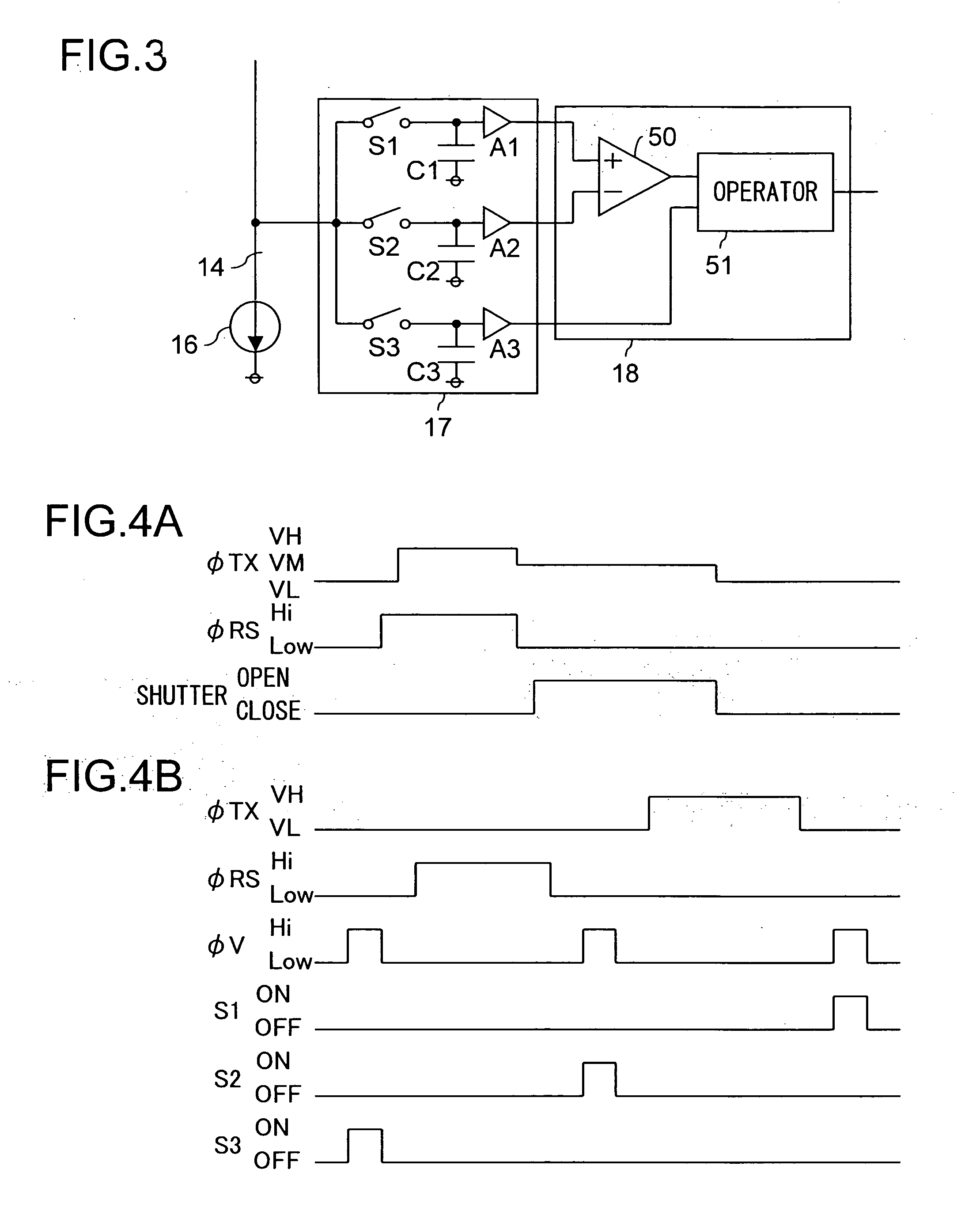
[0033] In the i...


PUM


Abstract

An image signal, a noise signal, and an overflow signal outputted from a solid-state image-sensing device are sampled-and-held in capacitors C1, C2, and C3 in a sample-and-hold circuit 17. Thereafter, the image signal and the noise signal in the capacitors C1 and C2 are fed to a subtractor 50 in a correction circuit 18, so that the image signal having noise eliminated therefrom is fed to an operator 51. In this operator 51, according to the value of the overflow signal in the capacitor C3, the image signal having noise eliminated therefrom is corrected by adding thereto an integrated component.

Description

[0001] This application is based on Japanese Patent Application No. 2005-248592 filed on Aug. 30, 2005 and Japanese Patent Application No. 2006-144218 filed on May 24, 2006, the contents of both of which are hereby incorporated by reference. BACKGROUND OF THE INVENTION [0002] 1. Field of the Invention [0003] The present invention relates to a solid-state image-sensing device provided with pixels that output electrical signals commensurate with incident light, and more particularly to a solid-state image-sensing device of which the pixels are built with transistors. [0004] 2. Description of Related Art [0005] Finding many uses, solid-state image-sensing devices are largely classified into a CCD type and a CMOS type according to the means they use to read (extract) photoelectric charges produced by photoelectric conversion elements. In a CCD-type solid-state image-sensing device, photoelectric charges are transferred while being accumulated in potential wells. This leads to a disadvan...

Claims


Application Information

Patent Timeline
Patent Type & Authority Applications(United States)
IPC IPC(8): H04N5/335H04N5/355H04N5/369H04N5/374H04N5/376H04N5/378
CPCH04N5/335H01L27/14609H04N25/00
Inventor KAKUMOTO, TOMOKAZU
Owner KONICA MINOLTA INC
Why Eureka
Try Eureka