Method for manufacturing display and display

a technology of display and display, applied in the manufacture of electrode systems, electric discharge tubes/lamps, discharge tubes luminescnet screens, etc., can solve the problems of contact failure between the upper electrode and the auxiliary electrode, deteriorating display performance, and difficult to enhance display performance, etc., to achieve the effect of lowering the aperture ratio and low aperture ratio

Inactive Publication Date: 2008-02-28
JOLED INC
View PDF5 Cites 30 Cited by
  • Summary
  • Abstract
  • Description
  • Claims
  • Application Information

AI Technical Summary

Benefits of technology

[0012]As a countermeasure to prevent this problem, a method would be available in which the lower electrode and the auxiliary electrode are disposed at positions that are sufficiently far away from each other so that the laser light irradiation area will not overlap with the auxiliary electrode. However, this method imposes severe limitations on the pixel layout, and leads to a low aperture ratio.
[0013]There is a need for the present invention to provide a method in which in formation of an organic layer on a lower electrode by a contact transfer method, formation of the organic layer on an auxiliary electrode can be prevented without the lowering of the pixel aperture ratio.

Problems solved by technology

Therefore, a voltage gradient is generated in the upper electrode and thus a voltage drop arises therein, which significantly deteriorates the displaying performance.
However, when the above-described contact transfer method is applied to manufacturing of a display in which an auxiliary electrode is provided, if an error of the laser light irradiation position occurs, an organic layer will be transferred also onto the auxiliary electrode, which will cause contact failure between the upper electrode and the auxiliary electrode.
This precludes the effective prevention of the voltage drop, and thus makes it difficult to enhance the displaying performance.
However, this method imposes severe limitations on the pixel layout, and leads to a low aperture ratio.

Method used


Image

  • Method for manufacturing display and display
  • Method for manufacturing display and display
  • Method for manufacturing display and display

Examples


first embodiment

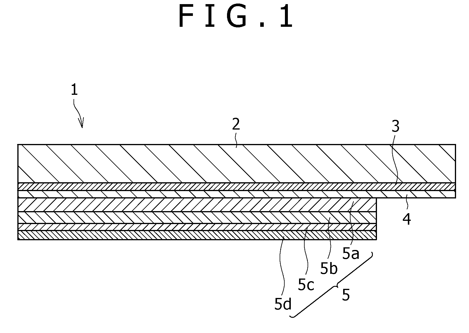
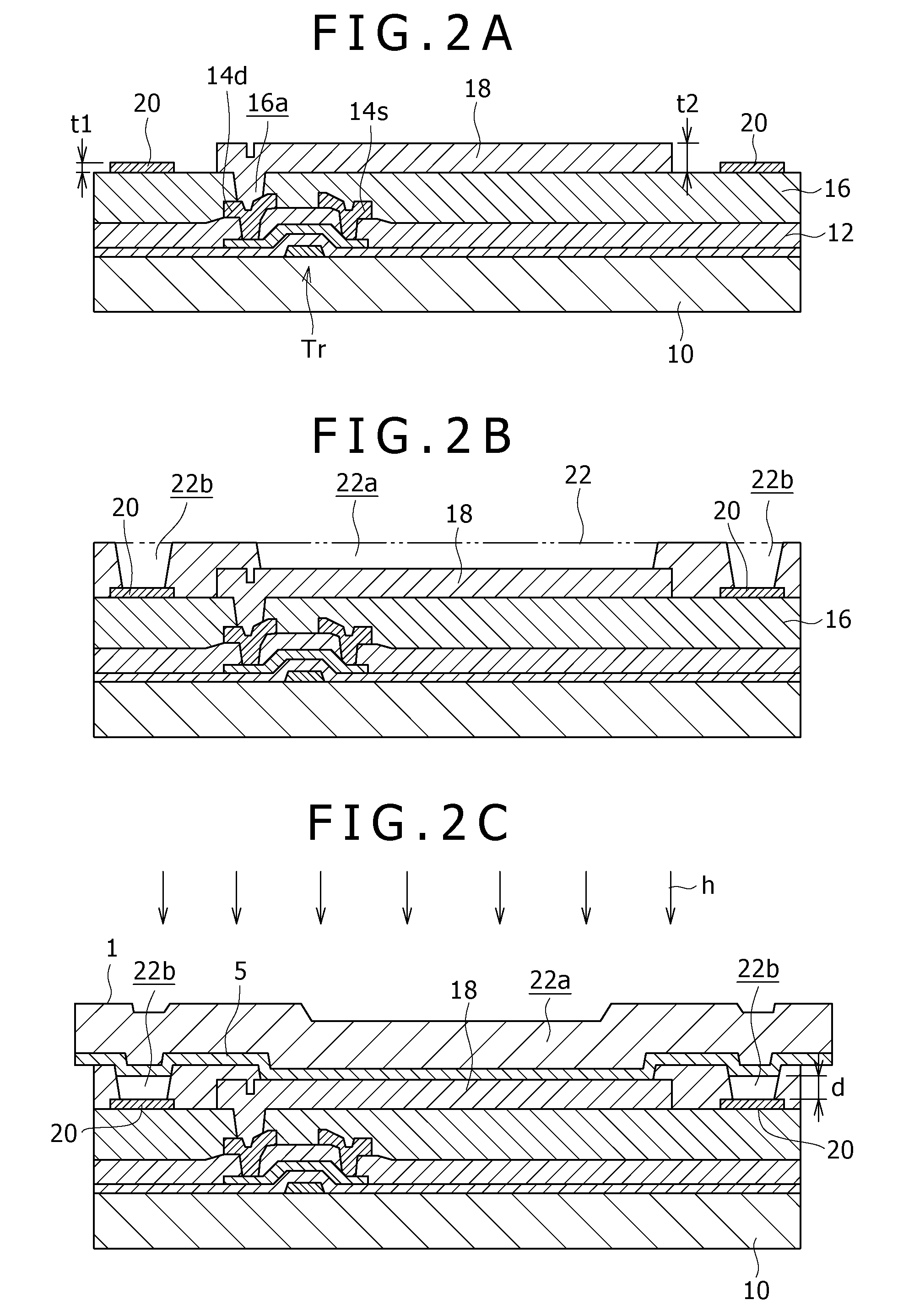
[0037]FIGS. 2A to 2F are sectional views for explaining steps of a manufacturing method that employs a donor film having the above-described one configuration example according to a first embodiment of the present invention. These sectional views of steps correspond to a section of one pixel in the display area.

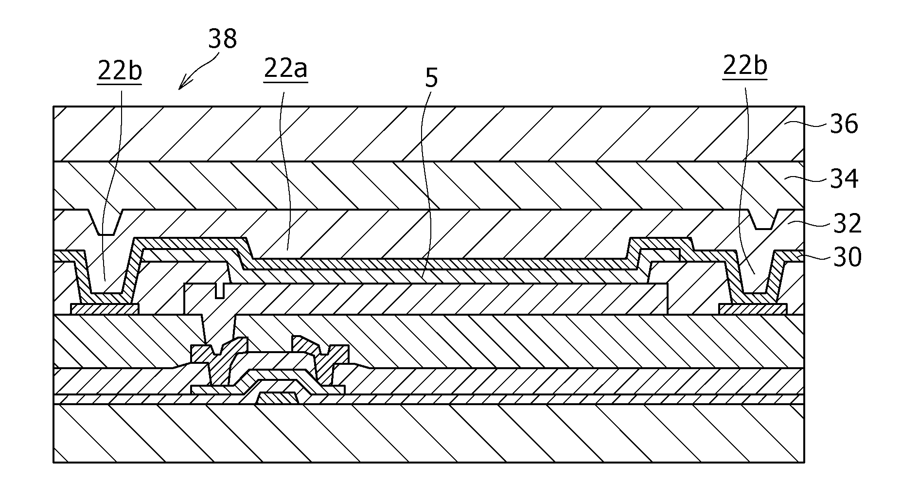
[0038]Referring initially to FIG. 2A, a thin film transistor Tr, capacitive element, and resistive element (not shown) included in a pixel circuit are formed on a substrate 10 composed of e.g. an optically transparent material. Subsequently, a first insulating film 12 that covers these elements (thin film transistor Tr, in the drawing) is deposited. Furthermore, on the first insulating film 12, a source electrode interconnect 14s and a drain electrode interconnect 14d that are connected to the transistor Tr, and a signal line, power supply line, and so on that are connected to these interconnects 14s and 14d are adequately formed.

[0039]Thereafter, a second insulating film 16 ...

second embodiment

[0070]FIGS. 4A to 4F are sectional views for explaining steps of a manufacturing method that employs a donor film having the above-described one configuration example according to a second embodiment of the present invention. These sectional views of steps correspond to a section of one pixel in the display area. The same components in the second embodiment as those in the first embodiment are given the same numerals, and a redundant description thereof is omitted.

[0071]Referring initially to FIG. 4A, elements such as a thin film transistor Tr included in a pixel circuit are formed on a substrate 10, and these elements are covered by a first insulating film 12. On the first insulating film 12, a source electrode interconnect 14s and a drain electrode interconnect 14d that are connected to the thin film transistor Tr, and a signal line, power supply line, and so on that are connected to these interconnects 14s and 14d are adequately formed.

[0072]Subsequently, a second insulating film...

third embodiment

[0083]FIGS. 5A to 5F are sectional views for explaining steps of a manufacturing method that employs a donor film having the above-described one configuration example according to a third embodiment of the present invention. These sectional views of steps correspond to a section of one pixel in the display area. The same components in the third embodiment as those in the second embodiment are given the same numerals, and a redundant description thereof is omitted.

[0084]Referring initially to FIG. 5A, elements such as a thin film transistor Tr included in a pixel circuit are formed on a substrate 10, and these elements are covered by a first insulating film 12. On the first insulating film 12, a source electrode interconnect 14s and a drain electrode interconnect 14d that are connected to the thin film transistor Tr, and a signal line, power supply line, and so on that are connected to these interconnects 14s and 14d are adequately formed.

[0085]Subsequently, similarly to the second e...


PUM


Abstract

Disclosed herein is a method for manufacturing a display, the method including the steps of: disposing a substrate over which a plurality of lower electrodes and a plurality of auxiliary electrodes are formed and a donor film over which a light-emitting functional layer is formed so that the light-emitting functional layer contacts with the lower electrodes and does not contact with the auxiliary electrodes; irradiating the donor film with an energy beam to selectively transfer the light-emitting functional layer onto the lower electrodes; and forming an upper electrode that covers the light-emitting functional layer and the auxiliary electrodes.

Description

CROSS REFERENCES TO RELATED APPLICATIONS[0001]The present invention contains subject matter related to Japanese Patent Application JP 2006-226003 filed in the Japan Patent Office on Aug. 23, 2006, the entire contents of which being incorporated herein by reference.BACKGROUND OF THE INVENTION[0002]1. Field of the Invention[0003]The present invention relates to a method for manufacturing a display that has organic electro-luminescence elements each including an organic light-emitting layer, and a display.[0004]2. Description of the Related Art[0005]An organic electro-luminescence element, which employs electro-luminescence (hereinafter, represented as EL) of an organic material, is a light-emitting element that includes a light-emitting layer composed of an organic material and so on between a lower electrode and an upper electrode and can emit light with high luminance through low-voltage DC driving.[0006]In recent years, attention is being paid on a transfer method as a technique fo...

Claims


Application Information

Patent Timeline
Patent Type & Authority Applications(United States)
IPC IPC(8): H01L27/32H01J9/00
CPCH01L27/3244H01L51/56H01L51/5228H10K59/12H10K50/824H10K71/00H05B33/10
Inventor MATSUDA, EISUKE
Owner JOLED INC
Why Eureka
Try Eureka