Semiconductor device having metal gate and manufacturing method thereof

a technology of semiconductor devices and manufacturing methods, which is applied in the direction of semiconductor devices, electrical devices, transistors, etc., can solve the problems of high thermal budget and impact on the process of metal gate, and improve the performance of transistor devices, and achieve high thermal budget

Active Publication Date: 2015-12-24
UNITED MICROELECTRONICS CORP
View PDF11 Cites 0 Cited by
  • Summary
  • Abstract
  • Description
  • Claims
  • Application Information

AI Technical Summary

Benefits of technology

[0011]According to the semiconductor device having metal gate and the manufacturing method thereof provided by the present invention, the metal-last process is integrated with the epitaxy technique. Accordingly, the epitaxial channel layer is formed in the gate trench after performing steps having high thermal budget such as source / drain formation, and silicide process. And the metal gate is subsequently formed in the gate trench. Since the epitaxial channel layer and the metal gate are all formed after process requiring high temperature, qualities of the metal gate and the epitaxial channel layer are no longer impacted by those processes and thus performance of the transistor device is improved.

Problems solved by technology

It is observed that processes with high thermal budget impacts not only the metal gate process, but also the quality of the epitaxial layers.

Method used


Image

  • Semiconductor device having metal gate and manufacturing method thereof
  • Semiconductor device having metal gate and manufacturing method thereof
  • Semiconductor device having metal gate and manufacturing method thereof

Examples


Embodiment Construction

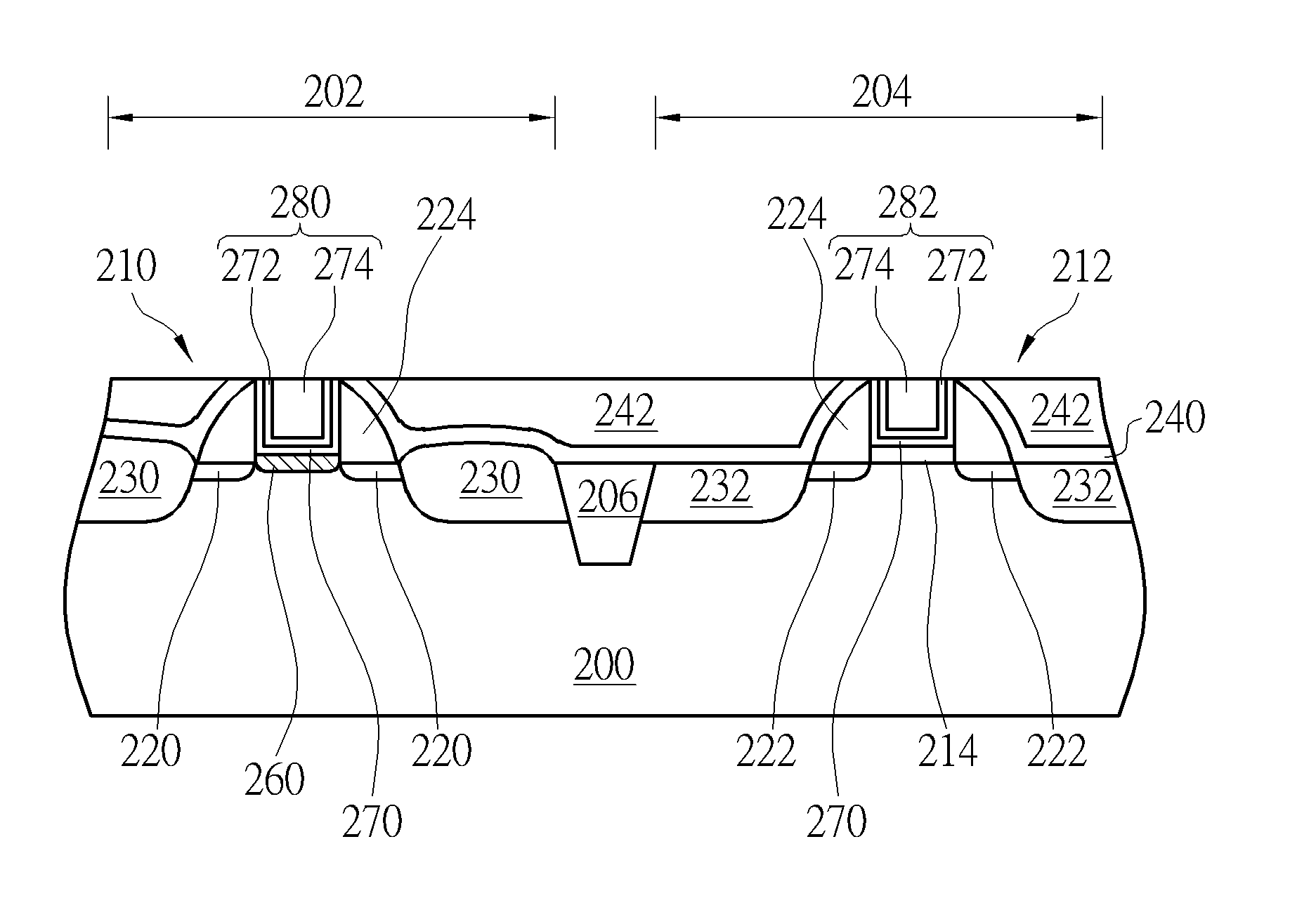
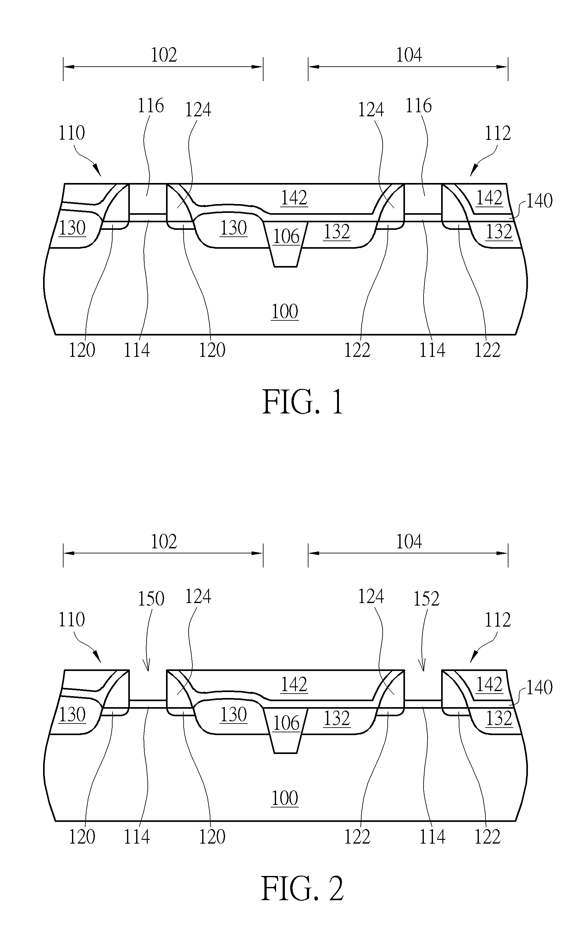
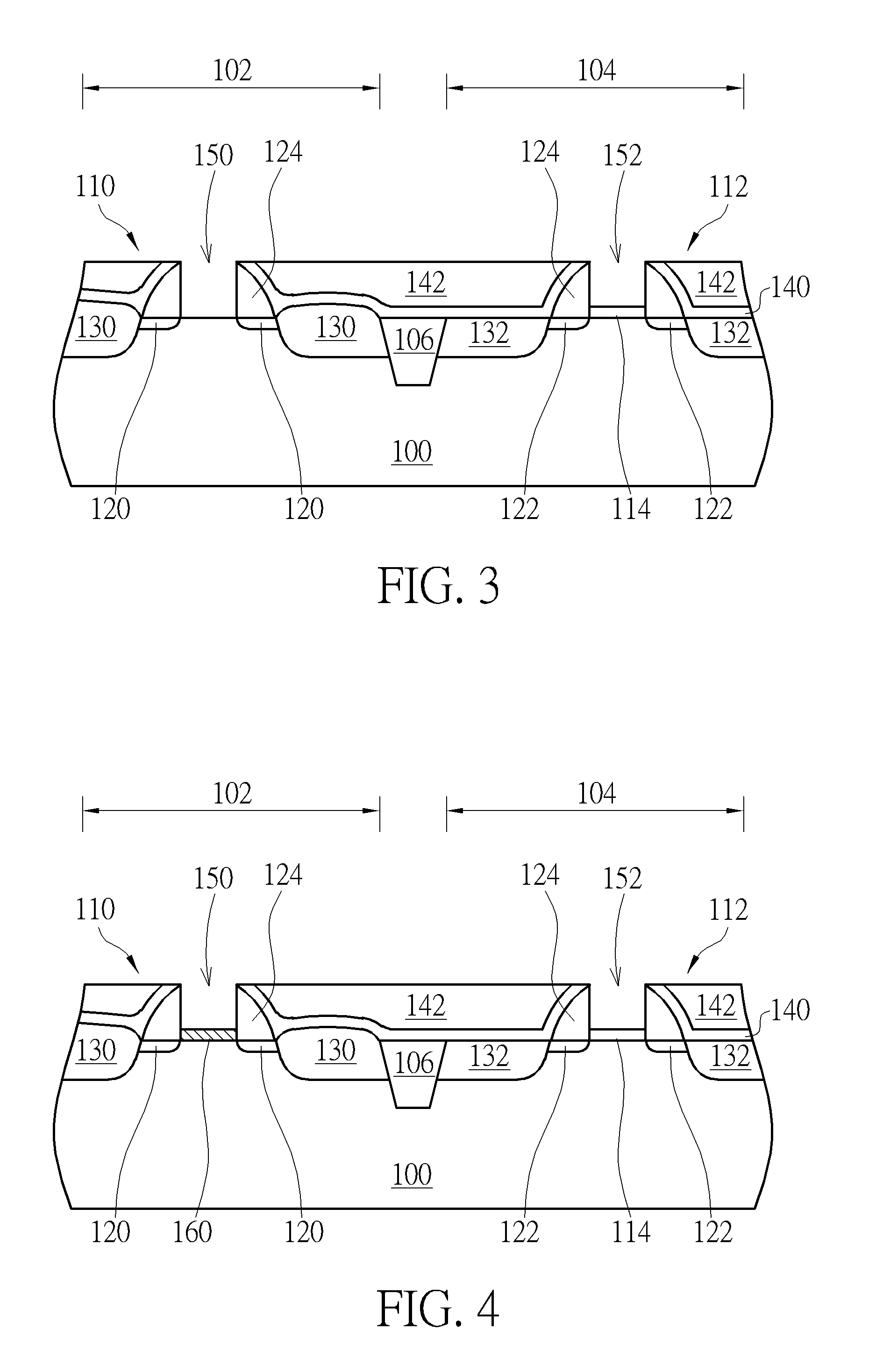
[0023]Please refer to FIGS. 1-6, which are drawings illustrating a manufacturing method for a semiconductor device having metal gate provided by a first preferred embodiment of the present invention. As shown in FIG. 1, the preferred embodiment first provides a substrate 100 such as silicon substrate, silicon-containing substrate, or silicon-on-insulator (SOI) substrate. The substrate 100 includes a core region 102 and a peripheral region 104 defined thereon. An isolation structure 106, such as a shallow trench isolation (STI) is formed in the substrate 100 between the core region 102 and the peripheral region 104 for rendering electrical isolation. A first semiconductor device 110 is formed in the core region 102 and a second semiconductor device 112 is formed in the peripheral region 104. In the preferred embodiment, the first semiconductor device 110 and the second semiconductor device 112 include the same conductivity type. However, those skilled in the art would easily realize ...


PUM


Abstract

A semiconductor device having metal gate includes a substrate, a metal gate positioned on the substrate, a high-k gate dielectric layer, and an epitaxial channel layer positioned in between the high-k gate dielectric layer and the substrate. A length of the epitaxial channel layer is larger than a length of the metal gate, and a bottom of the epitaxial channel layer and the substrate are coplanar.

Description

CROSS REFERENCE TO RELATED APPLICATIONS[0001]This is a continuation application of U.S. patent application Ser. No. 13 / 943,721, filed on Jul. 16, 2013, and all benefits of such earlier application are hereby claimed for this new continuation application.BACKGROUND OF THE INVENTION[0002]1. Field of the Invention[0003]The invention relates to a semiconductor device having metal gate and manufacturing method thereof, and more particularly, to a semiconductor device having metal gate and manufacturing method integrated with epitaxy technique.[0004]2. Description of the Prior Art[0005]With semiconductor processes entering the era of the deep submicron meter, it has been more and more important to increase the metal-oxide semiconductor (MOS) drive current. To improve device performance, epitaxy technique is developed to enhance carrier mobility of the channel region.[0006]On the other hands, with the trend toward scaling down the size of the semiconductor device, work function metals are ...

Claims


Application Information

Patent Timeline
Patent Type & Authority Applications(United States)
IPC IPC(8): H01L29/49H01L29/78H01L29/16H01L29/20H01L29/51H01L29/423
CPCH01L21/823807H01L21/823857H01L29/66545H01L29/6659H01L29/66636H01L29/66651H01L29/7848H01L29/517H01L21/823828H01L29/16H01L29/20H01L29/42364H01L29/495H01L29/4966
Inventor HOU, YONG TIAN
Owner UNITED MICROELECTRONICS CORP
Why Eureka
Try Eureka