Method for producing a conductive nanoparticle memory device

a nanoparticle memory and nanoparticle technology, applied in nanoinformatics, instruments, coatings, etc., can solve the problems of revealing defects in said dielectric, reducing the thickness of the dielectric, and reducing the dimension of the memory devi

Inactive Publication Date: 2013-03-05
COMMISSARIAT A LENERGIE ATOMIQUE ET AUX ENERGIES ALTERNATIVES +1
View PDF12 Cites 0 Cited by
  • Summary
  • Abstract
  • Description
  • Claims
  • Application Information

AI Technical Summary

Benefits of technology

[0011]Thus there is a need to propose a method for producing a memory device not having the drawbacks of the prior art, which is compatible with the steps of a CMOS method, in other words not requiring a high thermal budget, and which makes it possible to obtain a better control of the size of the electron storage sites, as well as a higher density of electron storage sites in the memory device.

Problems solved by technology

Such a floating gate memory device has several drawbacks when it is sought to miniaturise it.
Indeed, the reduction in the dimensions of this device necessarily entails reducing the thickness of the dielectric that insulates the floating gate from the substrate.
This reduction in thickness of said dielectric leads to problems of retention of information by the memory device because the electrons stored in the floating gate can exit it much more easily by tunnel effect.
In addition, this reduction in the thickness of the dielectric reveals defects in said dielectric, said defects favouring the leakage of electrons as the information writing cycles are carried out in the memory device.
Just one of these defects may for example completely empty the floating gate of the electrons that are stored therein.
The nanocrystals are formed of an implantation of silicon or germanium in the control oxide then an annealing at a temperature equal to around 950° C. Such a production method nevertheless has the major drawbacks of:requiring a high thermal budget, incompatible with the other steps of producing the device when it is wished to produce the memory device by a standard CMOS method,being inefficient as to the precipitation of implanted atoms into nanocrystals.
In addition, these techniques do not enable densities of nanocrystals greater than around 1012 cm−2 to be obtained.

Method used


Image

  • Method for producing a conductive nanoparticle memory device
  • Method for producing a conductive nanoparticle memory device
  • Method for producing a conductive nanoparticle memory device

Examples


first embodiment

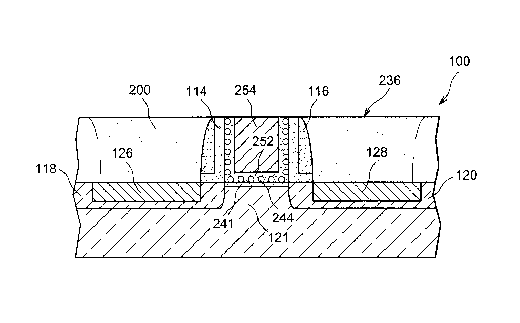
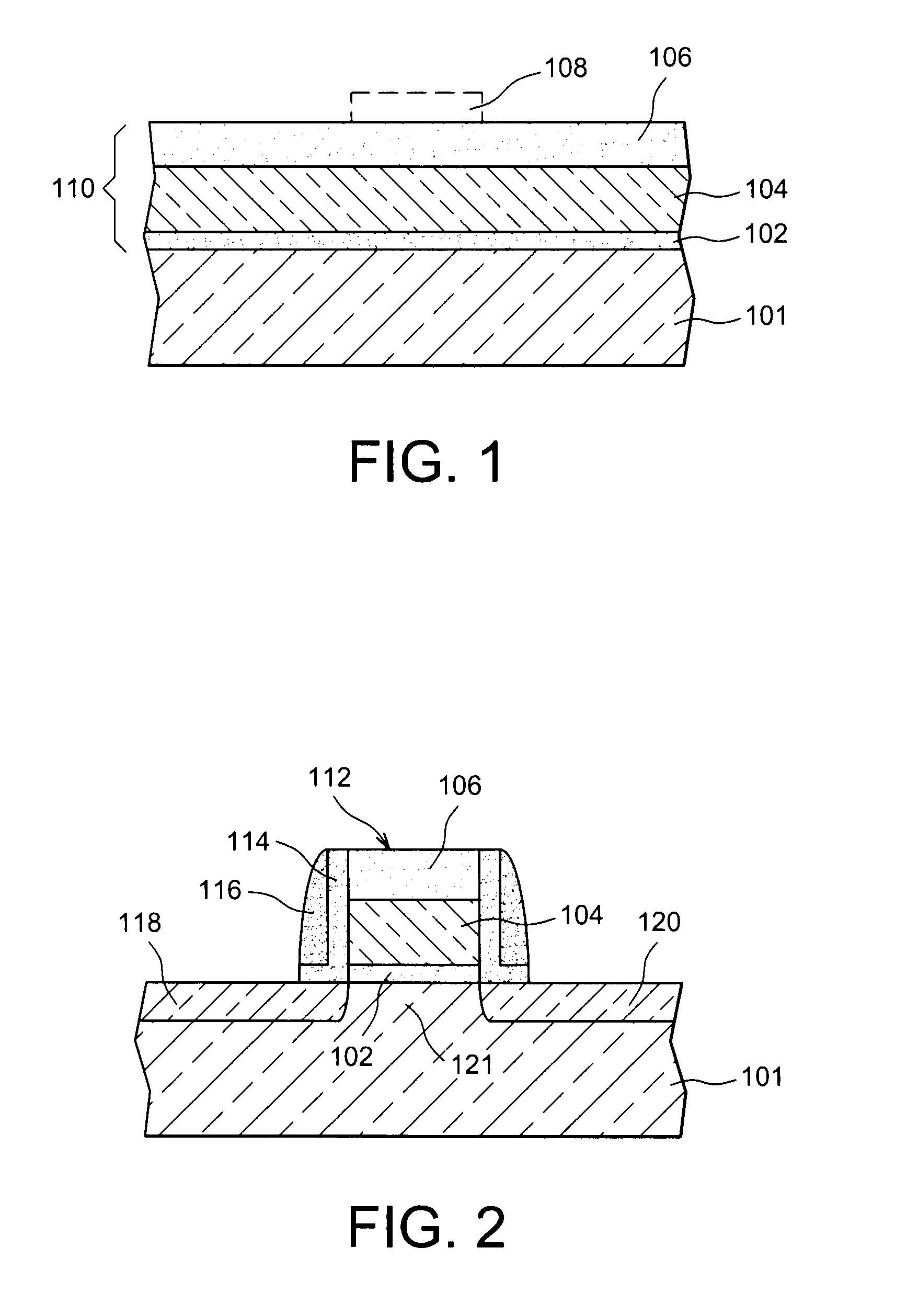
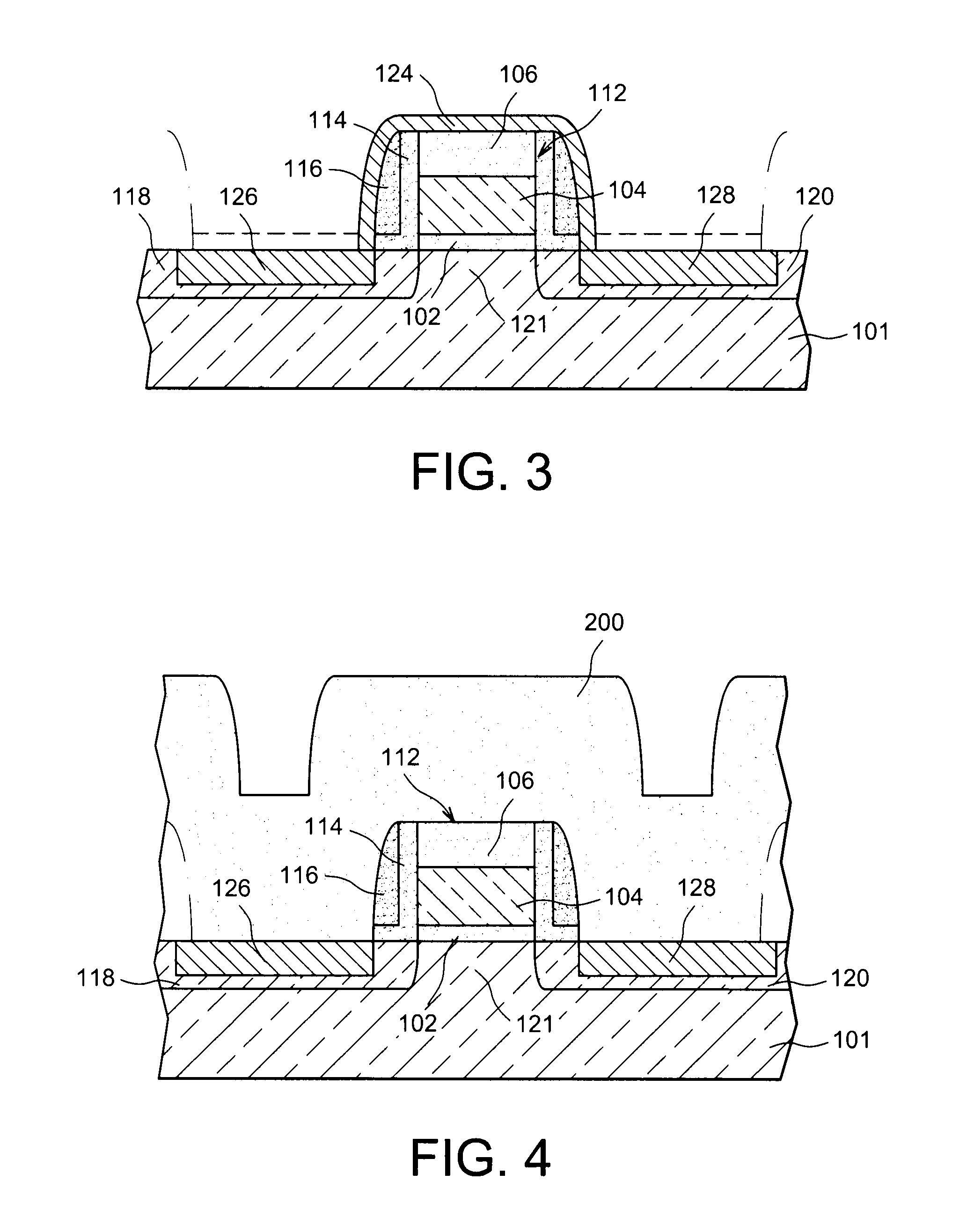
[0050]FIGS. 1 to 9 represent the steps of a method for producing a nanoparticle memory device

second embodiment

[0051]FIGS. 10 and 11 represent a nanoparticle memory device obtained by the implementation of a method for producing a nanoparticle memory device

third embodiment

[0052]FIG. 12 represents a nanoparticle memory device obtained by the implementation of a method for producing a nanoparticle memory device according to a

[0053]Identical, similar or equivalent parts of the different figures described hereafter bear the same numerical references so as to make it easier to go from one figure to the next.

[0054]In order to make the figures easier to read, the different parts represented in the figures are not necessarily to the same scale.

[0055]The different possibilities (alternatives and embodiments) must be understood as not being mutually exclusive and may be combined together.


PUM


Abstract

A method for producing a memory device with nanoparticles, including steps of: a) forming, in a substrate based on at least one semi-conductor, source and drain regions, and at least one first dielectric on at least one zone of the substrate arranged between the source and drain regions and intended to form a channel of the memory device, b) depositing of at least one ionic liquid that is an organic salt or mixture of organic salts in a liquid state, wherein nanoparticles of at least one electrically conductive material are suspended in the ionic liquid, said ionic liquid covering at least said first dielectric, c) forming a deposition of said nanoparticles at least on said first dielectric, d) removing the ionic liquid remaining on the first dielectric, and e) forming at least one second dielectric and at least one control gate on at least one part of the nanoparticles deposited on the first dielectric.

Description

TECHNICAL FIELD[0001]This document relates to the field of electronic memories and the production of such memories. More specifically, it relates to the production of an electronic or microelectronic memorisation device, or memory device, of non-volatile type, in other words which conserves data in the absence of electrical supply, with electrically conductive nanoparticles, for example of Flash type.STATE OF THE PRIOR ART[0002]It is generally sought to produce memories or memory circuits with ever increasing information storage capacities and reading and writings speeds. These objectives entail miniaturising the electronic components forming these memories and increasing the integration densities of these components.[0003]A conventional floating gate memory device, in other words an individual electronic memorisation component, has a structure similar to that of a field effect transistor, in other words it comprises a source, a channel and a drain. Nevertheless, compared to a field...

Claims


Application Information

Patent Timeline
Patent Type & Authority Patents(United States)
IPC IPC(8): H01L21/336
CPCB82Y10/00H01L21/28273H01L29/42332H01L29/66825H01L29/7881H01L29/66833H01L27/11563H01L29/513H01L29/66545Y10S977/773B82Y40/00H01L29/40114H10B43/00
Inventor DELEONIBUS, SIMONBASSET, JEAN-MARIECAMPBELL, PAULGUTEL, THIBAUTHAUMESSER, PAUL-HENRIMARCHAND, GILLESSANTINI, CATHERINE
Owner COMMISSARIAT A LENERGIE ATOMIQUE ET AUX ENERGIES ALTERNATIVES
Why Eureka
Try Eureka