Method of manufacturing an electronic device

a manufacturing method and electronic device technology, applied in the field of microelectronic devices, can solve the problems of degrading the functionality revealing limitations in the current technique, and unable to meet the requirements of the desired structure, and achieves stable final stack, high electrical continuity, and effective bonding

Active Publication Date: 2021-05-13
COMMISSARIAT A LENERGIE ATOMIQUE ET AUX ENERGIES ALTERNATIVES
View PDF17 Cites 0 Cited by
  • Summary
  • Abstract
  • Description
  • Claims
  • Application Information

AI Technical Summary

Benefits of technology

[0019]Thus, effective bonding is obtained with high electrical continuity between the substrate and the silicon carbide-based layer. This ensures a stable final stack even at high temperature with strong vertical electrical conductivity.
[0020]While the presence of tungsten silicide layer(s) could a priori have appeared to be unfavourable to the conductivity of the stack produced, relative to tungsten alone in particular, this controlled presence (these layers are intentionally manufactured, therefore in particular of reduced and adjustable thicknesses without technical difficulty) allows, contrary to this prejudice, to obtain a stable stack in terms of composition, because little or not sensitive to the diffusion of species during technological steps with a high thermal budget; all this while ensuring good vertical conductivity from an electrical point of view.
[0023]Such a device provides a stack of layers favourable to subsequent technological steps, in particular when high temperatures are involved. The electrical conductivity through the stack is improved, in particular with respect to stacks without resorting to tungsten and to silicides of this metal.
[0026]Thus, unlike patent application EP3229260A1 and thanks to the portions of diffusion barriers, a high thermodynamic stability is guaranteed, for example but in a non-limiting manner, up to a temperature range of at least 1900° C., and possibly between 25° C. and 1900° C. Indeed, the existence of a diffusion barrier portion formed of at least one tungsten silicide layer between the first metal layer and the primary layer and of a diffusion barrier portion formed of at least one tungsten silicide layer between the second metal layer and the substrate contributes to the method allowing to obtain thermodynamically stable structures while having a satisfactory level of electrical conductivity.

Problems solved by technology

The technical constraints of this method for placing silicon carbide layers with bonding are nevertheless very severe.
In this context, the current technique reveals limitations, in particular through the formation of chemical phases degrading the functionality of the desired structure: liquid phase, parasitic solid phase, cavities, etc.
However, this method does not seem to allow to guarantee high thermodynamic stability, for example up to a temperature range of at least 1900° C.

Method used


Image

  • Method of manufacturing an electronic device
  • Method of manufacturing an electronic device

Examples


Embodiment Construction

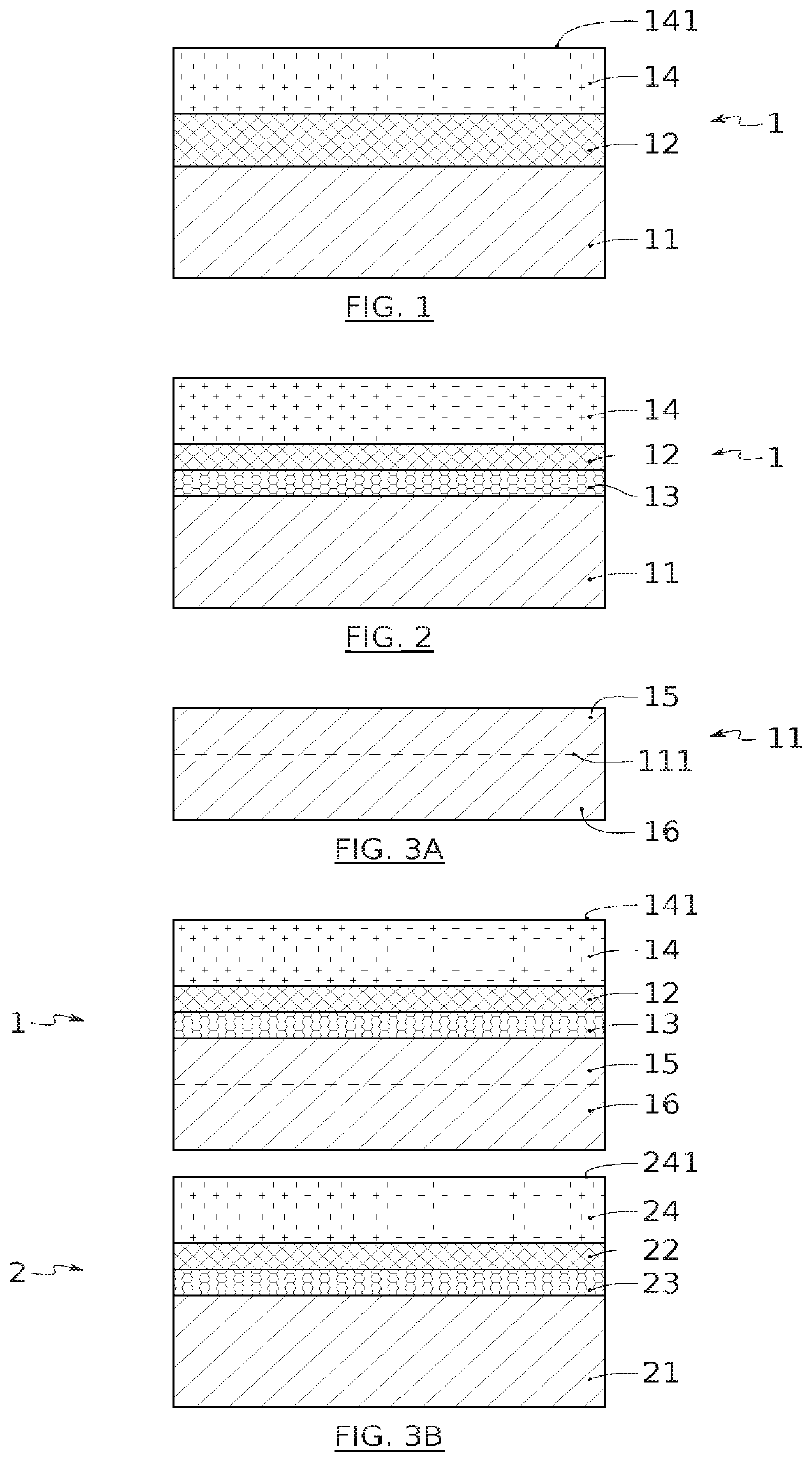
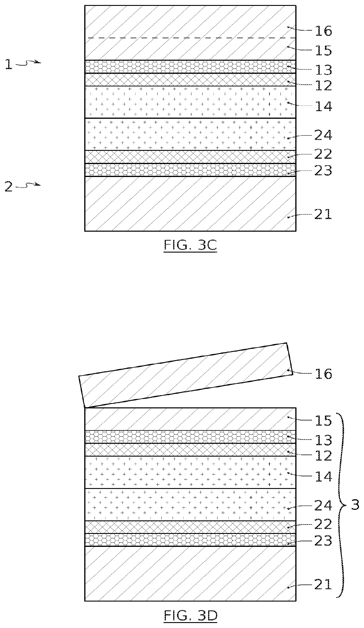
[0032]Before starting a detailed review of embodiments of the invention, optional features are listed below which can optionally be used in combination or alternatively:[0033]at least one of the tungsten silicide layers is a layer of a material selected from WSi2 and W5Si3;[0034]the first portion is formed of at least one W5Si3 layer 12.[0035]the W5Si3 layer 12 of the first portion is in contact with the first metal layer 14;[0036]the first portion is also formed of a WSi2 layer 13 between the primary layer 11 and the W5Si3 layer 12 of the first portion;[0037]the second portion is formed of at least one W5Si3 layer 22.[0038]the W5Si3 layer 22 of the second portion is in contact with the second metal layer 24;[0039]the second portion is also formed of a WSi2 layer 23 between the substrate 21 and the W5Si3 layer 22 of the second portion;[0040]at least one tungsten silicide layer of at least one of the first portion and the second portion is selected with a thickness less than or equal...


PUM

PropertyMeasurementUnit
thicknessaaaaaaaaaa
temperatureaaaaaaaaaa

Abstract

There is provided a method for manufacturing an electronic device including a substrate of semiconductor material, an intermediate portion, and a silicon carbide layer, the method including transferring the silicon carbide layer from a first electronic element onto a face of a second electronic element including the substrate, the transfer including: providing the first element including a primary silicon carbide-based layer, a first diffusion barrier portion, and a first metal layer; providing the second element including the substrate, a second diffusion barrier portion, and a second metal layer; and bonding an exposed face of each of the first and the second metal layers, the first and the second metal layers being formed of tungsten, the first and the second portions being formed of at least one tungsten silicide layer, and the second portion, the second metal layer, the first metal layer, and the first portion form the intermediate portion.

Description

TECHNICAL FIELD[0001]The present invention relates to the field of electronics in general and microelectronic devices. It finds a particularly advantageous application in the field of power transistors, this example not being limiting. Any application implementing silicon carbide and requiring vertical electrical conductivity is open to the invention.[0002]In general, the invention can be used in all microelectronic devices.PRIOR ART[0003]In the case of power transistors operating vertically (that is to say according to the thickness dimension of the substrates), a bonding of semiconductor materials with a buried conductive layer is of major interest for micro-electronic applications. In order to achieve this assembly, a technical solution is the placement of thin films of monocrystalline silicon carbide (SiC) onto a substrate, in particular made of polycrystalline silicon carbide, via an electrically conductive bonding.[0004]It is in this context that the patent publication U.S. Pa...

Claims


Application Information

Patent Timeline
Patent Type & Authority Applications(United States)
IPC IPC(8): H01L21/02H01L23/00H01L29/16
CPCH01L21/02167H01L24/29H01L24/83H01L2224/29684H01L29/1608H01L2224/83895H01L2924/01074H01L24/27H01L21/185H01L21/0485H01L21/02002
Inventor NASER, HASAN
Owner COMMISSARIAT A LENERGIE ATOMIQUE ET AUX ENERGIES ALTERNATIVES
Why Eureka
Try Eureka