Method for manufacturing photo mask and photo mask manufactured with same

a manufacturing method and technology for photo masks, applied in the field of liquid crystal display, can solve the problems of difficult positioning and fixing, increased installation time, and relatively high manufacture cost, and achieve the effect of reducing mass differences

Active Publication Date: 2016-01-14
SHENZHEN CHINA STAR OPTOELECTRONICS TECH CO LTD
View PDF4 Cites 4 Cited by
  • Summary
  • Abstract
  • Description
  • Claims
  • Application Information

AI Technical Summary

Benefits of technology

[0010]An object of the present invention is to provide a method for manufacturing a photo mask, which applies half etching to an ineffective area in order to reduce mass difference between an effective open area and an adjacent ineffective area

Problems solved by technology

However, since it is thin, it is difficult to position and fix, the installation being more time-consuming and the manufacture cost being relatively high.
However, since the effective open areas 100 are provided with a plurality of vapor deposition apertures, the mass of an effective open area 100 and the mass of an ineffective area bet

Method used


Image

  • Method for manufacturing photo mask and photo mask manufactured with same
  • Method for manufacturing photo mask and photo mask manufactured with same
  • Method for manufacturing photo mask and photo mask manufactured with same

Examples


Embodiment Construction

[0041]To further expound the technical solution adopted in the present invention and the advantages thereof, a detailed description is given to a preferred embodiment of the present invention and the attached drawings.

[0042]Referring to FIGS. 5-7, the present invention provides a method for manufacturing a photo mask, which comprises the following steps:

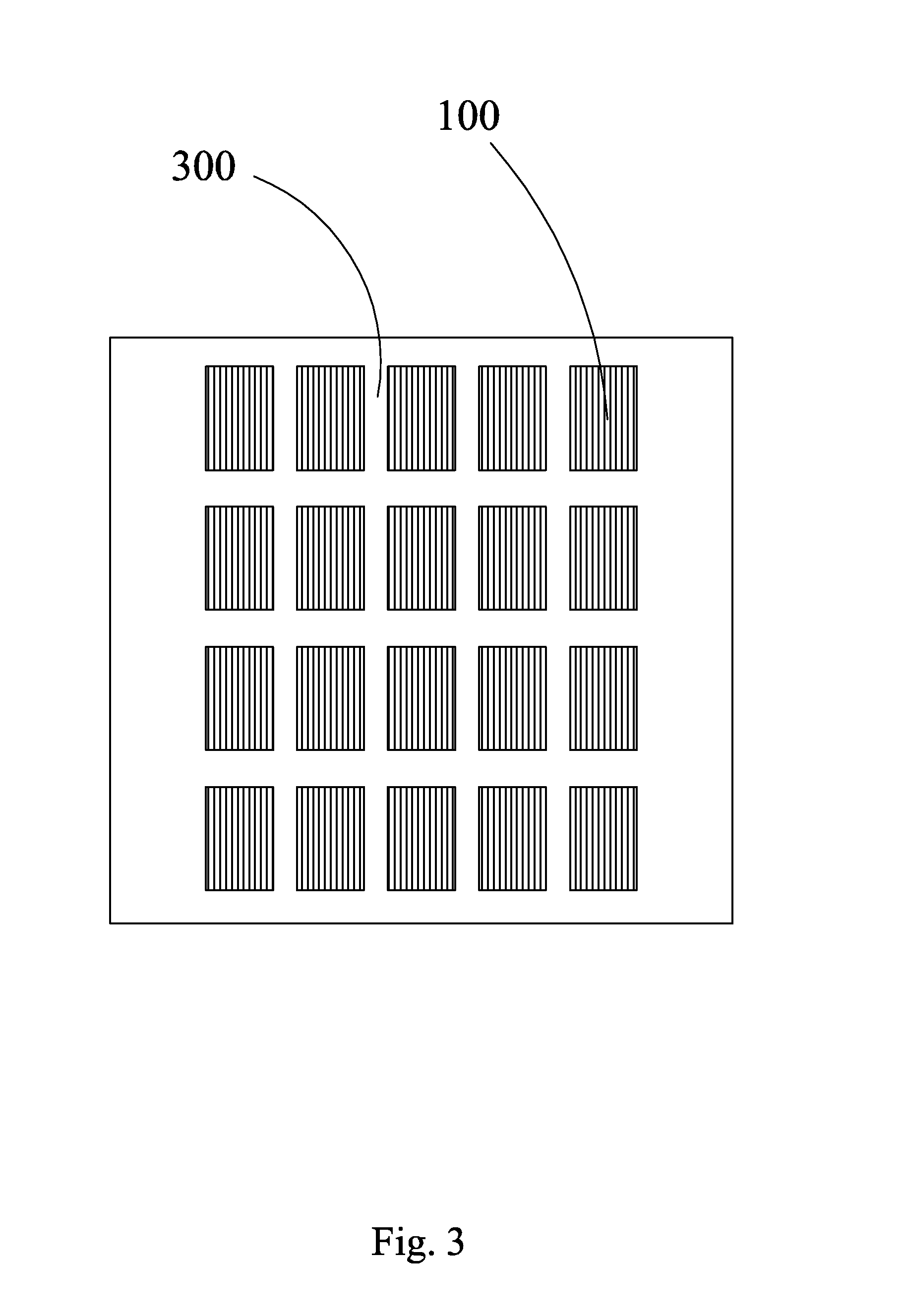
[0043]Step 1: providing a partially finished photo mask, wherein the partially finished photo mask comprises a plurality of effective open areas 22 and ineffective areas 24 located around the effective open areas 22.

[0044]The partially finished photo mask is provided by using a known technique and is made of a magnetic material. The partially finished photo mask can be for example a full sheet mask and a divide mask.

[0045]The effective open areas 22 are provided with a plurality of vapor deposition apertures 222 and the vapor deposition apertures 222 are arranged according to a desired deposition pattern.

[0046]Step 2: applying a half...


PUM


Abstract

Disclosed are a method for manufacturing a photo mask and a photo mask manufactured with the method. The method includes (1) providing a partially finished photo mask, which has effective open areas and ineffective areas located around the effective open areas and (2) applying a half-etching process to form recesses in the ineffective areas. With the recesses formed through a half-etching process in the ineffective areas located around the effective open areas, a mass difference between the effective open areas and the ineffective areas is reduced so that in the process of attracting the photo mask, inconsistent sequence of attraction caused by a great mass difference between the effective open areas and the ineffective areas can be eliminated to thereby ensure that the effective open areas of the photo mask can be laid completely flat on a substrate at predetermined locations and thus ensure the preciseness of a deposited pattern.

Description

BACKGROUND OF THE INVENTION[0001]1. Field of the Invention[0002]The present invention relates to the field of liquid crystal display, and in particular to a method for manufacturing a photo mask for vapor deposition of organic light-emitting display panel and a photo mask manufactured with the method.[0003]2. The Related Arts[0004]Flat panel display devices have a variety of advantages, such as thin device body, low power consumption, and being free of radiation, and are thus widely used. The flat panel display devices that are currently available include liquid crystal displays (LCDs) and organic light-emitting displays (OLEDs).[0005]Referring to FIG. 1, a currently available organic light-emitting display generally comprises: a glass substrate 900, a transparent conductive layer 902 formed on the glass substrate 900, a hole transporting layer (HTL) 904 formed on the transparent conductive layer 902, an organic emitting material layer (EML) 906 formed on the hole transporting layer...

Claims


Application Information

Patent Timeline
IPC IPC(8): G03F1/80G03F1/50
CPCG03F1/50G03F1/80
Inventor WU, TAIPI
Owner SHENZHEN CHINA STAR OPTOELECTRONICS TECH CO LTD
Why Eureka
Try Eureka