

Display panel and method for manufacturing the same
a technology of display panel and manufacturing method, which is applied in the direction of thermoelectric device junction materials, electrical apparatus, and semiconductor devices, etc., can solve the problems of time-consuming and labor-intensive replacement process of uv mask, and damage to organic film by ultraviolet rays, so as to save time (at least 6 hours)
- Summary
- Abstract
- Description
- Claims
- Application Information
AI Technical Summary
Benefits of technology
Problems solved by technology
Method used
Image

Examples
Embodiment Construction
[0035]The following embodiments are referring to the accompanying drawings for exemplifying specific implementable embodiments of the present invention.
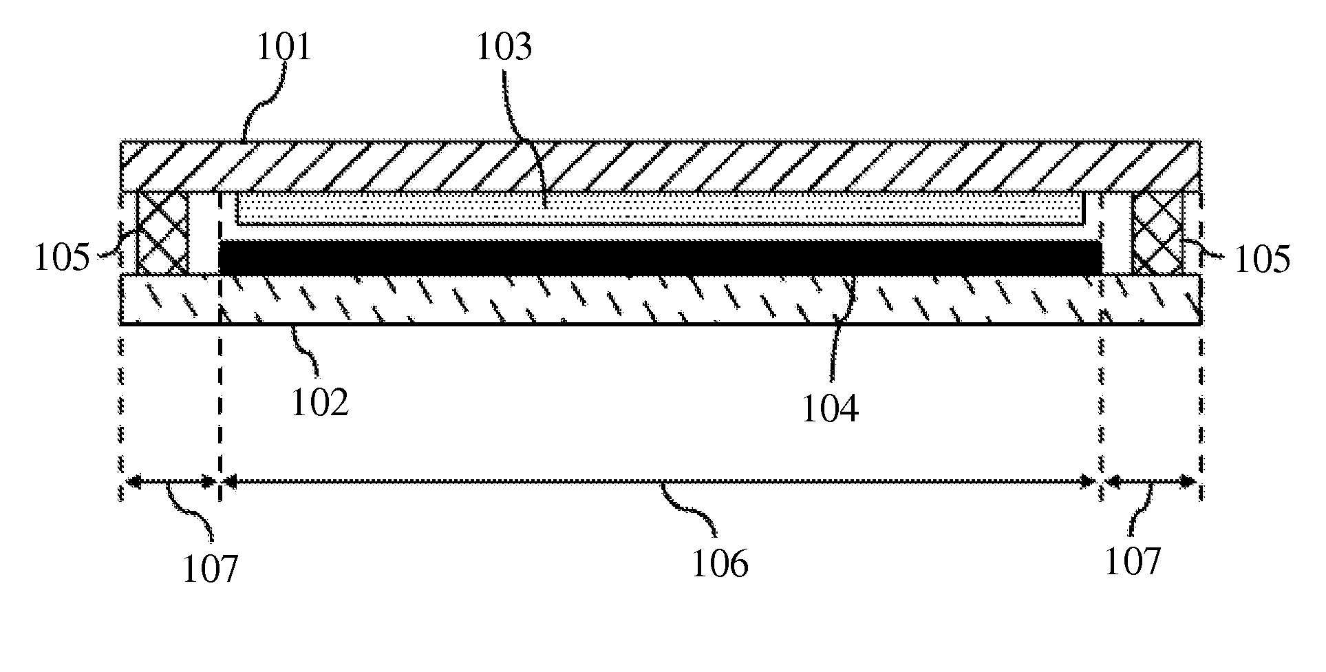
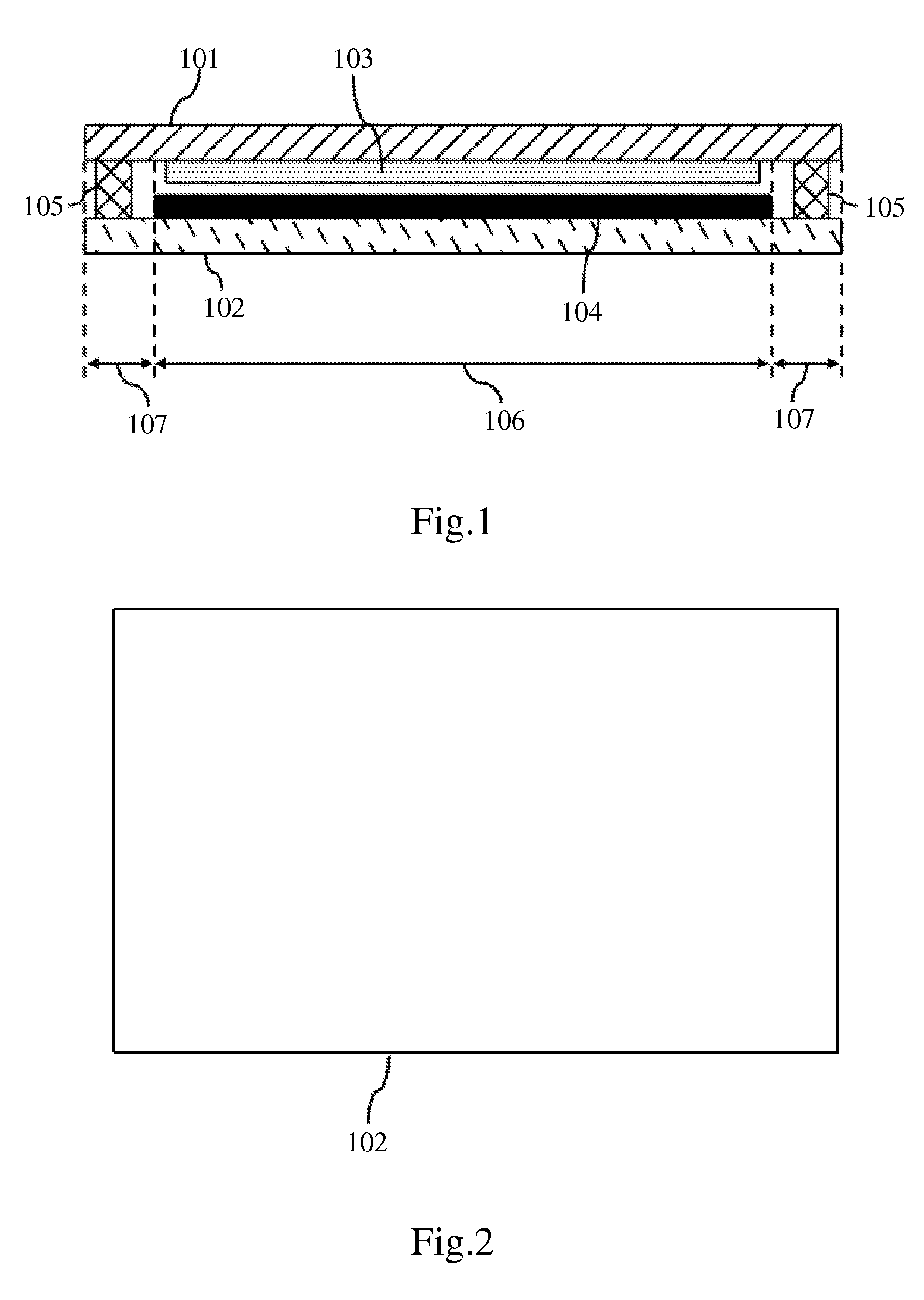
[0036]FIG. 1 is a schematic diagram showing a display panel according to an embodiment of the present invention.
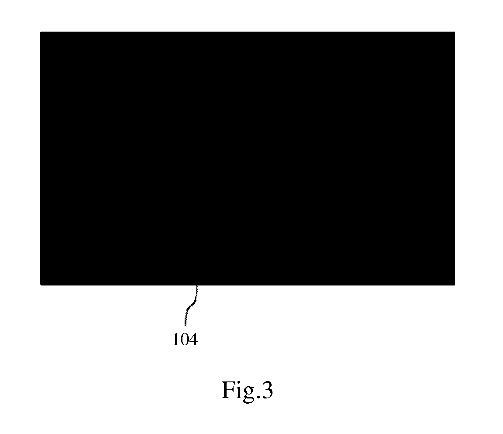
[0037]The display panel comprises a substrate 101, a cover 102, an OLED device 103, at least one shielding element 104, and at least one sealant 105.
[0038]The substrate 101 can be a transparent substrate (such as a glass substrate) and has a first surface, and the OLED device 103 is disposed on the first surface of the substrate 101. The OLED device 103 includes a cathode layer, an organic material layer, and an anode layer; the organic material layer is disposed between the cathode layer and the anode layer. The OLED device 103 is configured to display images when a voltage is applied to the organic material layer between the cathode layer and the anode layer, and the images can be shown from the transparent substrate.
[003...
PUM
 Abstract
Description
Claims
Application Information