Thin-film transistor substrate and display panel having the same

a thin-film transistor and substrate technology, applied in the field of photoalignment composition and a method of manufacturing a display panel, can solve the problem of difficult improvement of side visibility, and achieve the effects of preventing data signal delay, improving display quality, and reducing back channel field

Inactive Publication Date: 2016-01-28
SAMSUNG DISPLAY CO LTD
View PDF6 Cites 12 Cited by
  • Summary
  • Abstract
  • Description
  • Claims
  • Application Information

AI Technical Summary

Benefits of technology

[0030]In such embodiments, an organic insulating layer in a pixel area may be partially removed, so that a yellowish screen may be prevented, thereto improve a display quality. In addition, an organic insulating pattern may be formed on a data pattern including the data line, a source electrode and a drain electrode, a coupling capacitance between the data pattern and a common electrode may be prevented or decreased, thereto prevent a data signal delay. The organic insulating pattern may be formed on the thin film transistor to reduce back channel field effect.

Problems solved by technology

However, a liquid crystal display apparatus by PVA mode may have an after-image on a screen, and side visibility may be hard to improve.

Method used


Image

  • Thin-film transistor substrate and display panel having the same
  • Thin-film transistor substrate and display panel having the same
  • Thin-film transistor substrate and display panel having the same

Examples


Embodiment Construction

[0039]Hereinafter, exemplary embodiments of the inventive concept will be explained in detail with reference to the accompanying drawings.

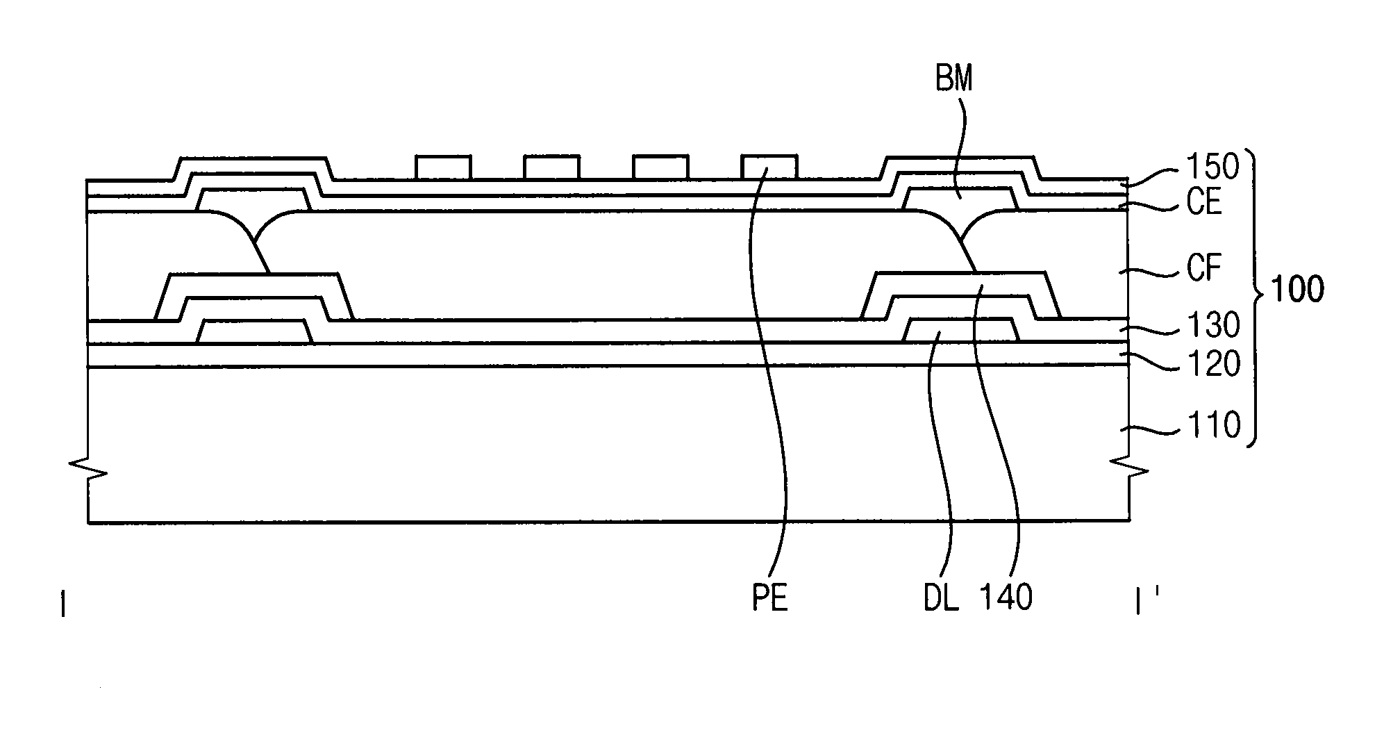
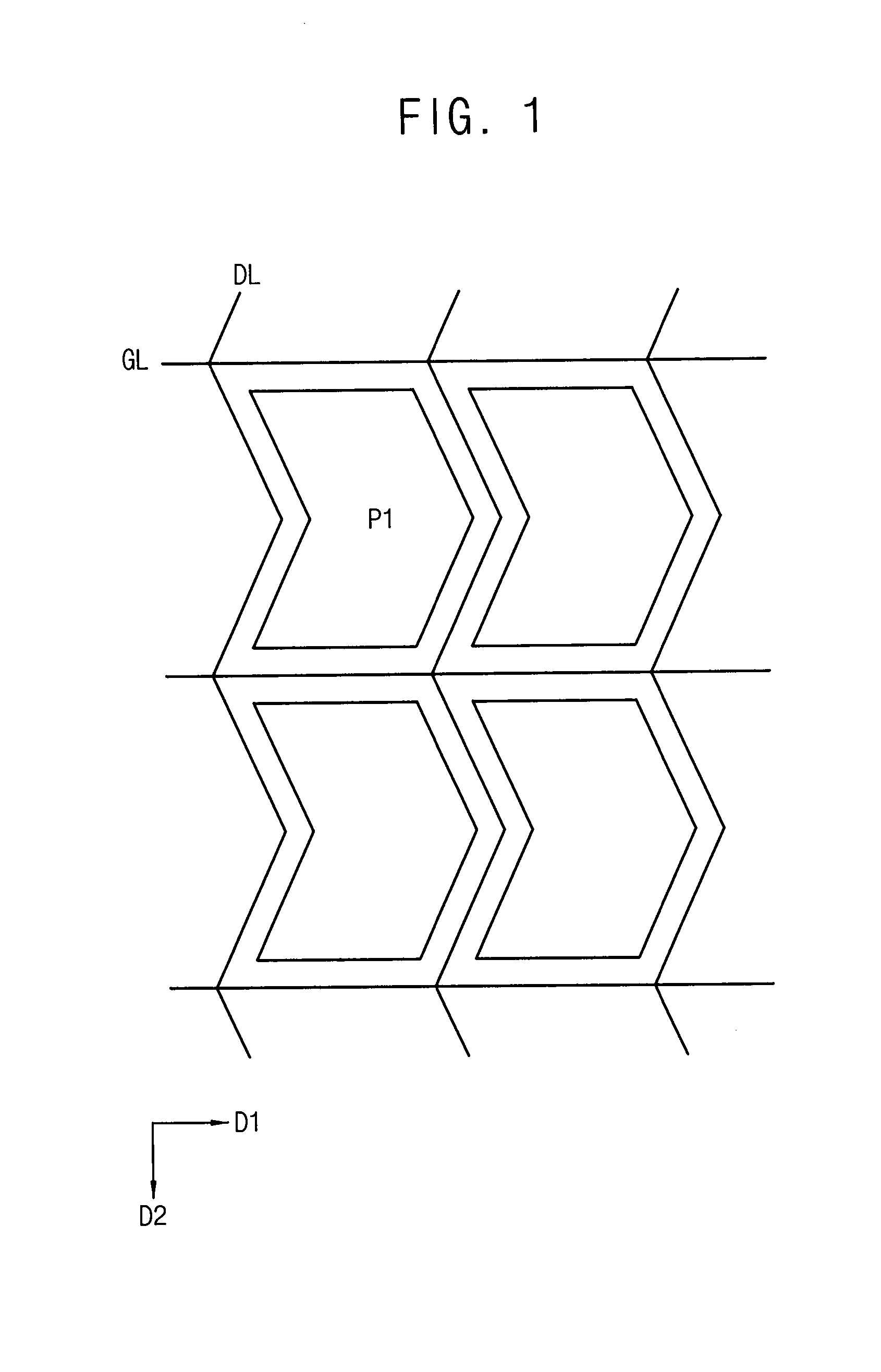
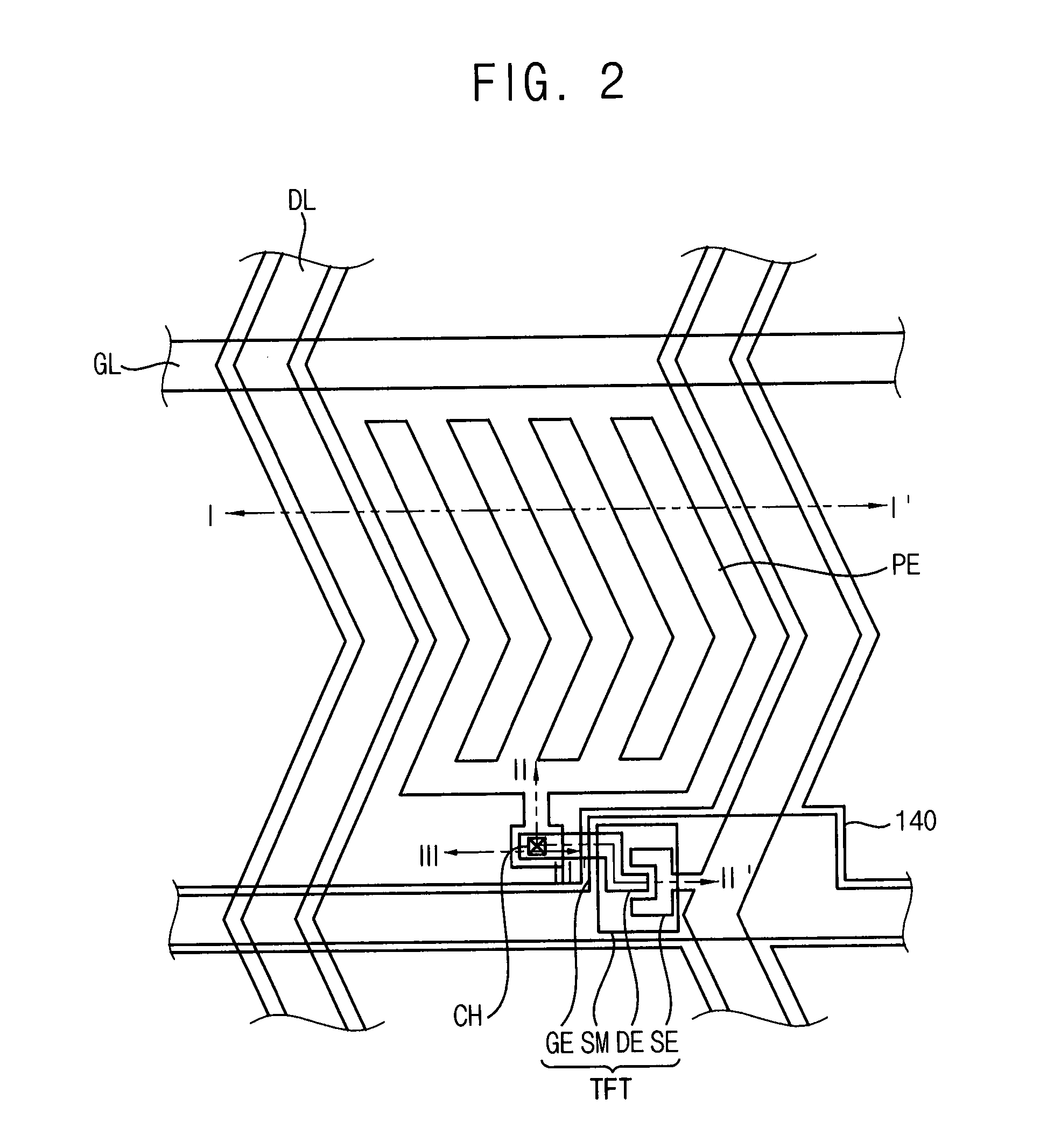
[0040]FIG. 1 is a plan view illustrating an exemplary embodiment of a display panel. FIG. 2 is a plan view illustrating an exemplary embodiment of a first pixel of FIG. 1. FIG. 3 is a cross-sectional view illustrating an exemplary embodiment of a display panel including a thin film transistor substrate taken along the line I-I′ of FIG. 2. FIG. 4 is a cross-sectional view illustrating an exemplary embodiment of the thin-film transistor substrate taken along the line I-I′ of FIG. 2.

[0041]FIG. 5 is a cross-sectional view illustrating an exemplary embodiment of a thin-film transistor substrate taken along the line II-II′ of FIG. 2. FIG. 6 is a cross-sectional view illustrating an exemplary embodiment of a thin-film transistor substrate taken along the line III-III′ of FIG. 2.

[0042]Referring to FIG. 1, the display panel includes a plurality of gate lin...


PUM

PropertyMeasurementUnit
thicknessaaaaaaaaaa
thicknessaaaaaaaaaa
photosensitiveaaaaaaaaaa

Abstract

A thin-film transistor substrate includes a base substrate, a gate line, a data line, a thin-film transistor, an organic insulating pattern and a common electrode. The base substrate includes a plurality of pixel areas. The gate line is disposed on the base substrate, and the gate line is extended in a first direction. The data line is disposed on the gate line, and the data line is extended in a second direction crossing the first direction. The thin-film transistor is connected to the gate line and the data line. The organic insulating pattern covers the data line and the thin-film transistor, and the organic insulating pattern includes an opening overlapping with the pixel areas. The common electrode is disposed on the base substrate. Thus, an organic insulating layer in a pixel area may be partially removed, so that a yellowish screen may be prevented, thereto improve a display quality. In addition, an organic insulating pattern may be formed on a data pattern, a coupling capacitance between the data pattern and a common electrode may be prevented or decreased, thereto prevent a data signal delay.

Description

CLAIM OF PRIORITY[0001]This application claims priority to Korean Patent Application No. 10-2014-0095892, filed on Jul. 28, 2014, and all the benefits accruing therefrom under 35 U.S.C. § 119, the contents of which are herein incorporated by reference in their entireties.BACKGROUND OF THE INVENTION[0002]1. Field of the Invention[0003]Exemplary embodiments of the inventive concept relate to a photo-alignment composition and a method of manufacturing a display panel using the same. More particularly, exemplary embodiments of the inventive concept relate to a photo-alignment composition capable of improving a hardness of an alignment layer and removing an afterimage of a display panel and a method of manufacturing a display panel using the photo-alignment composition.[0004]2. Description of the Related Art[0005]A liquid crystal display apparatus is one of a flat panel display FPD, which is used broadly recently. Examples of the flat panel display include, but are not limited to, a liqu...

Claims


Application Information

Patent Timeline
Patent Type & Authority Applications(United States)
IPC IPC(8): G02F1/1362G02F1/1368H01L27/12
CPCG02F1/136286H01L27/124G02F2001/136222G02F1/1368G02F1/136209H01L27/1248G02F1/133707G02F1/133788G02F1/133397G02F1/13606
Inventor PARK, SEUNG-HYUNSONG, JUN-HOSONG, JEAN-HO
Owner SAMSUNG DISPLAY CO LTD
Why Eureka
Try Eureka