Various stress free sensor packages using wafer level supporting die and air gap technique

a technology of wafer level supporting die and sensor package, applied in the field of semiconductor packaging, can solve the problem of reducing the size of the overall packag

Active Publication Date: 2016-03-03
APPLE INC
View PDF4 Cites 39 Cited by
  • Summary
  • Abstract
  • Description
  • Claims
  • Application Information

AI Technical Summary

Benefits of technology

[0006]Sensor packages and methods of formation are described. In an embodiment, a sensor package includes a supporting die characterized by a recess area and a support anchor protruding above the recess area. A sensor die is bonded to the support anchor such that an air gap exists between the sensor die and the recess area. The sensor die may be bonded to the support anchor in a single-sided support cantilever configuration such that a hanging area of the sensor die extends laterally from a contact area of the sensor die directly over the support anchor, and the air gap exists between the hanging area of the sensor die and the recess area. The sensor die includes a sensor positioned directly above the air gap. The sensor package may additionally include one or more stopper structures protruding above the recess area. In this manner, the stopper structures can provide structural integrity to the sensor package and protect the bond between the sensor die and supporting die from breaking due to excessive bending into the air gap. For example, the stopper structures and support anchor may be integrally formed. In an embodiment, the sensor is positioned entirely directly above the air cavity.

Problems solved by technology

As electronic products are becoming increasingly sophisticated and the size of the overall packages is reduced to meet market needs, these advances are associated with various packaging challenges to reduce cost and form factor of the packages.

Method used


Image

  • Various stress free sensor packages using wafer level supporting die and air gap technique
  • Various stress free sensor packages using wafer level supporting die and air gap technique
  • Various stress free sensor packages using wafer level supporting die and air gap technique

Examples


Embodiment Construction

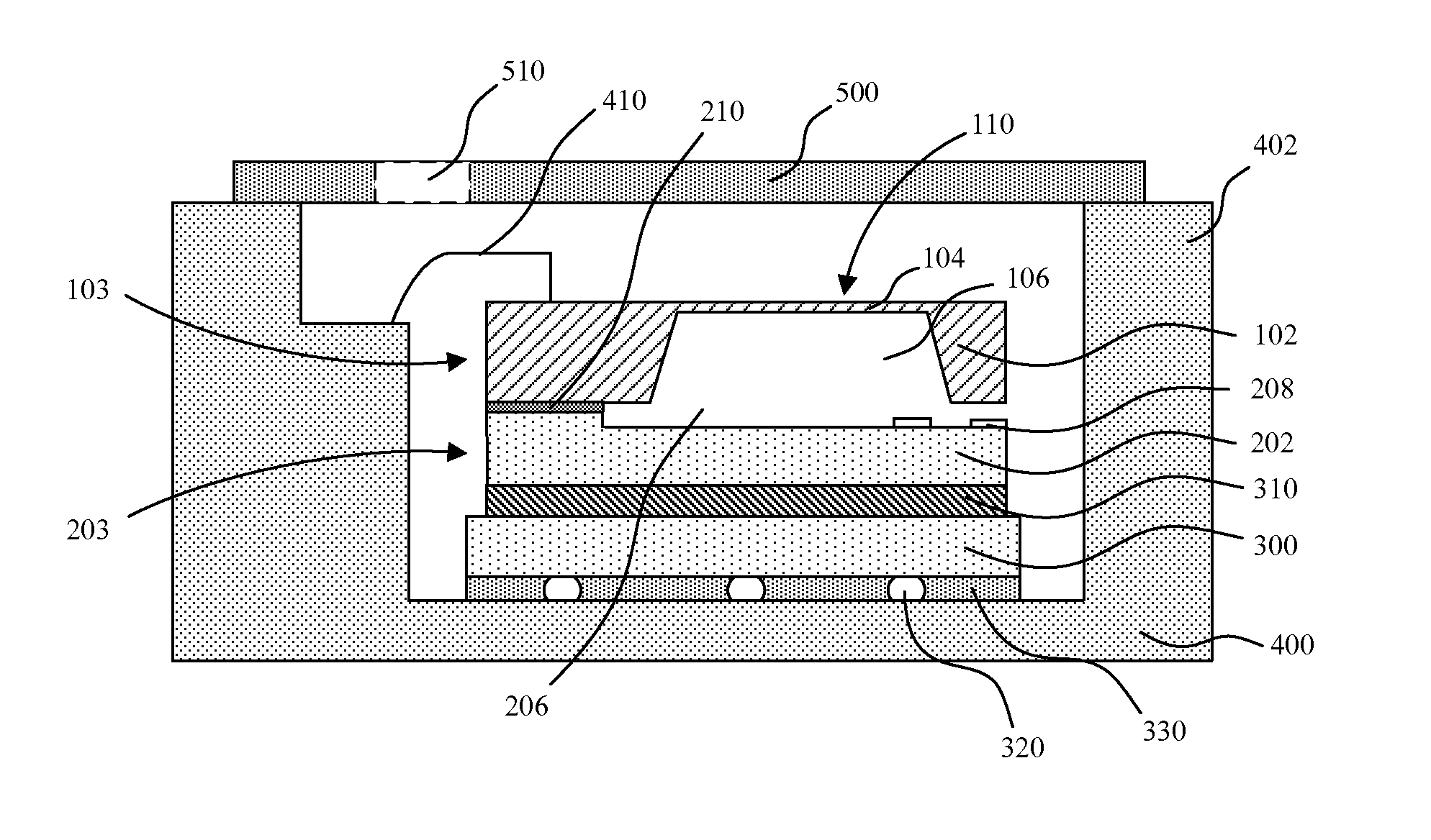
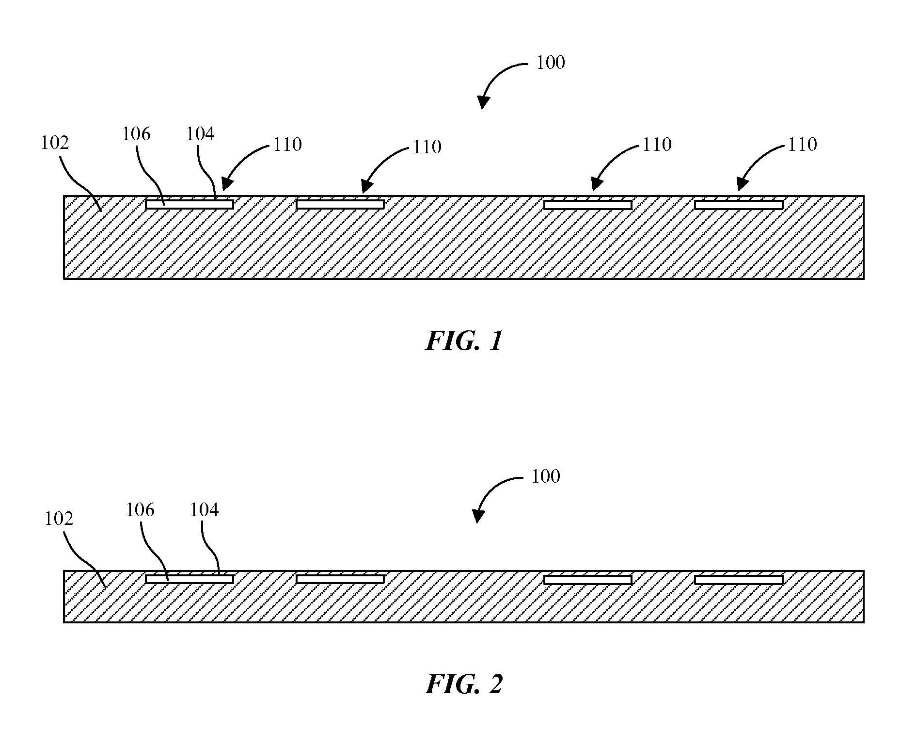
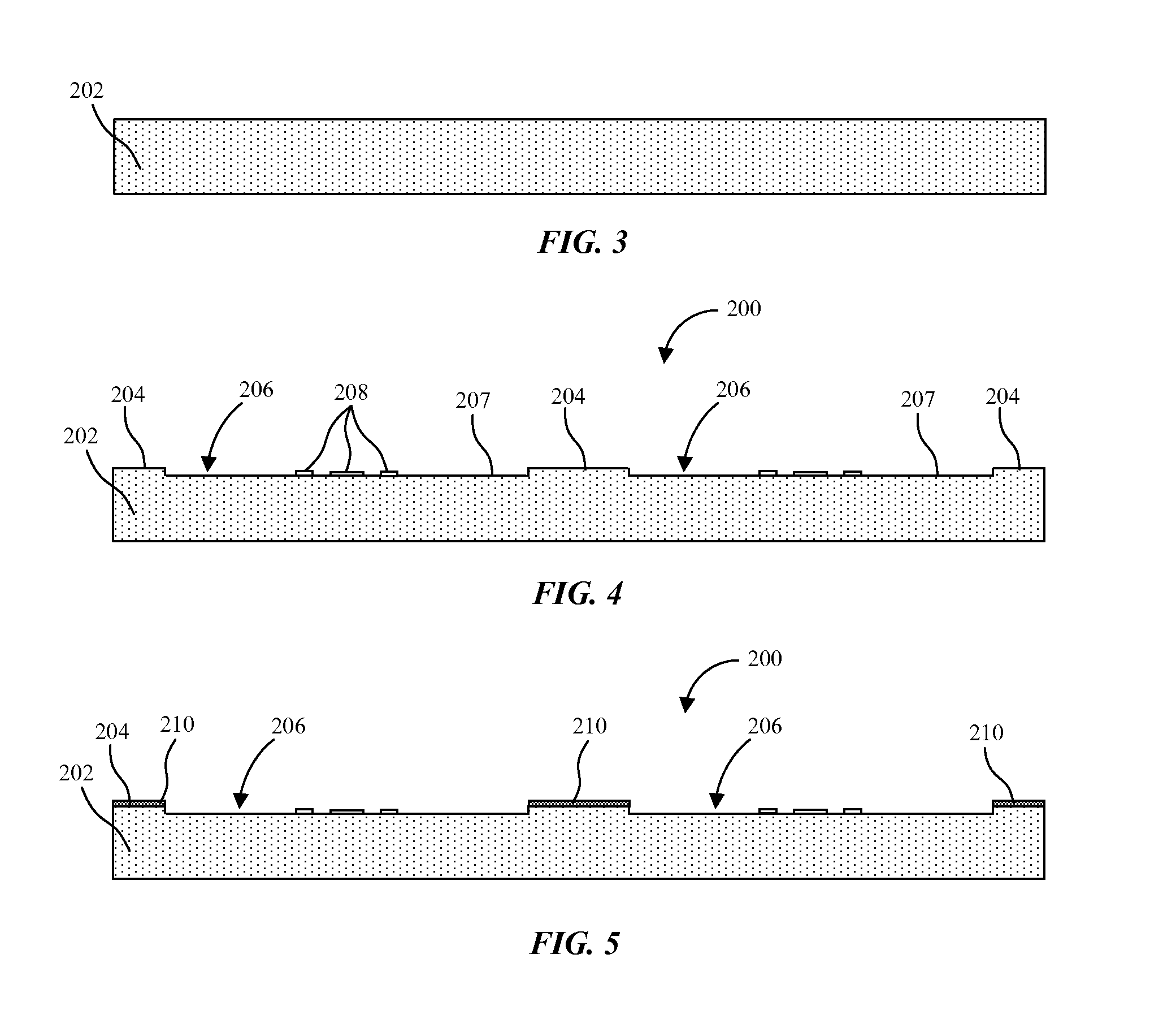
[0044]Embodiments describe sensor packages and methods of fabrication. In various embodiments, description is made with reference to figures. However, certain embodiments may be practiced without one or more of these specific details, or in combination with other known methods and configurations. In the following description, numerous specific details are set forth, such as specific configurations, dimensions and processes, etc., in order to provide a thorough understanding of the embodiments. In other instances, well-known semiconductor processes and manufacturing techniques have not been described in particular detail in order to not unnecessarily obscure the embodiments. Reference throughout this specification to “one embodiment” means that a particular feature, structure, configuration, or characteristic described in connection with the embodiment is included in at least one embodiment. Thus, the appearances of the phrase “in one embodiment” in various places throughout this spe...


PUM

PropertyMeasurementUnit
depthaaaaaaaaaa
recess areaaaaaaaaaaa
areaaaaaaaaaaa

Abstract

Sensor packages and manners of formation are described. In an embodiment, a sensor package includes a supporting die characterized by a recess area and a support anchor protruding above the recess area. A sensor die is bonded to the support anchor such that an air gap exists between the sensor die and the recess area. The sensor die includes a sensor positioned directly above the air gap.

Description

RELATED APPLICATIONS[0001]This application claims the benefit of priority from U.S. Provisional Patent Application Ser. No. 62 / 044,857 filed on Sep. 2, 2014, which is incorporated herein by reference.BACKGROUND[0002]1. Field[0003]Embodiments described herein relate to semiconductor packaging. More particularly embodiments relate to sensor packages and manners of fabrication.[0004]2. Background Information[0005]Sensor die can be formed from customized integrated circuits. Sensors are often used to sense environmental characteristics or act as a user input for electronic products. Sensors, unlike some general purpose integrated circuits, can have unique packaging and mounting requirements since sensors often require exposure to an ambient external environment, such as an ambient environment of a user using the electronic product having the sensor. As electronic products are becoming increasingly sophisticated and the size of the overall packages is reduced to meet market needs, these ...

Claims


Application Information

Patent Timeline
Patent Type & Authority Applications(United States)
IPC IPC(8): G01L7/08
CPCG01L7/08B81B7/0048H01L2224/16225H01L2224/32145H01L2224/48095H01L2224/73204H01L2224/73265H01L2224/94H01L2924/16151H01L2924/16195G01L9/0045G01L9/0048G01L19/0618G01L19/146G01L19/148H01L2924/1461H10N30/306H10N30/2042B81B2201/025B81B2201/0264B81B2203/0127B81B2203/0315B81B2207/012B81B2207/07B81B2207/094B81C1/0023B81C2203/0792
Inventor HAN, CALEB, C.JIANG, TONGBIZHAI, JUN
Owner APPLE INC
Why Eureka
Try Eureka