Unlock instant, AI-driven research and patent intelligence for your innovation.

Semiconductor device and information processing device

a technology of information processing and semiconductors, applied in the field of semiconductor devices, can solve problems such as the limitation of the types of ising models

Active Publication Date: 2016-03-03
HITACHI LTD
View PDF4 Cites 7 Cited by
  • Summary
  • Abstract
  • Description
  • Claims
  • Application Information

AI Technical Summary

Benefits of technology

The present invention provides a technique that enables the interaction calculations using the multi-valued coefficients of three or more values in a semiconductor device that carries out the calculation of an interaction model. This technique helps in improving the accuracy and efficiency of the device by using advanced calculations and optimizations. Overall, this invention helps in enhancing the performance and reliability of the semiconductor device.

Problems solved by technology

Also in the case of an Ising model, the interaction coefficients of spins are limited only to two values of +1 and −1, which therefore leads to the limitation of the types of the Ising model.

Method used


Image

  • Semiconductor device and information processing device
  • Semiconductor device and information processing device
  • Semiconductor device and information processing device

Examples


first embodiment

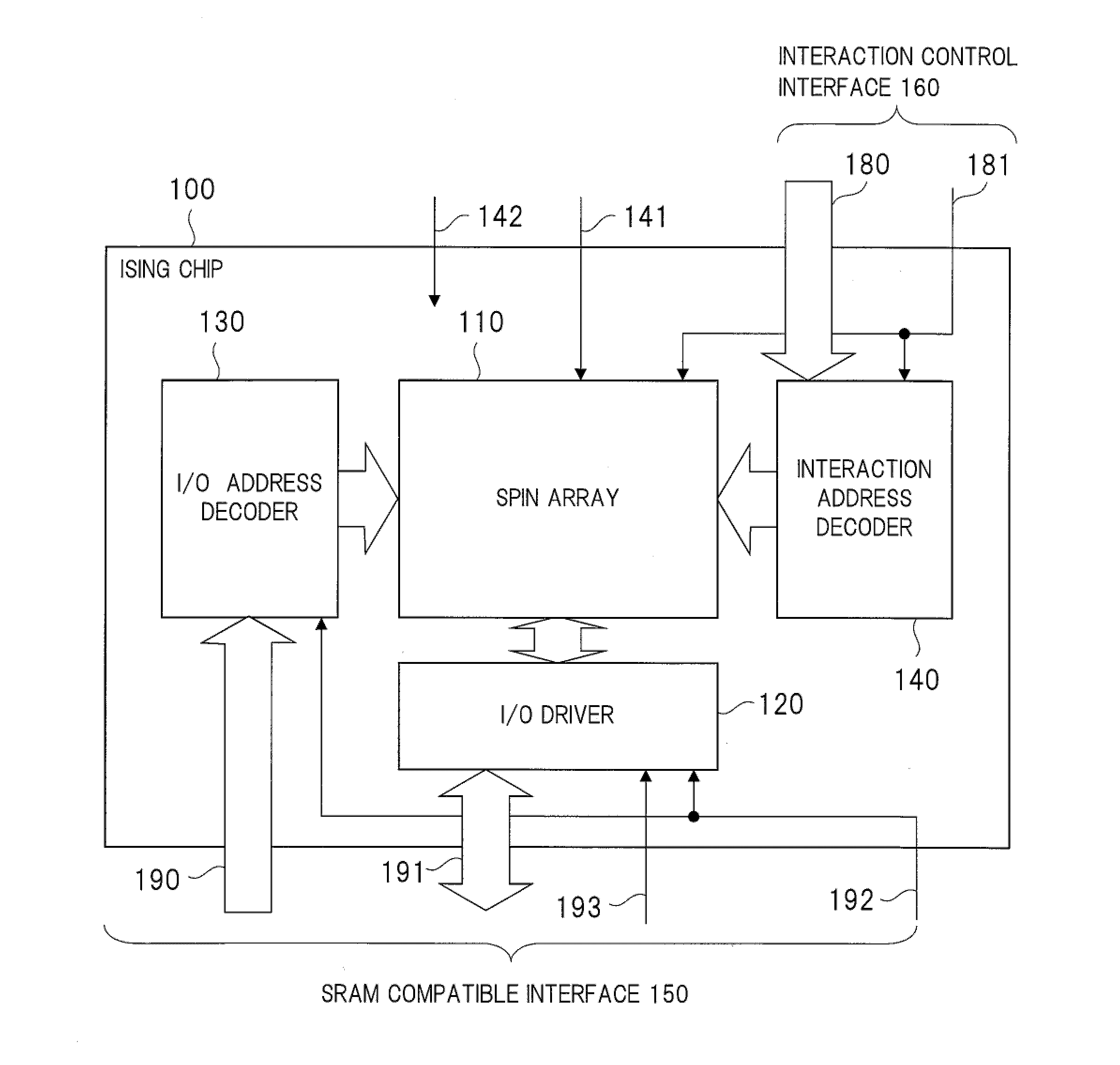
[0037]The present embodiment relates to a semiconductor device which carries out calculations of an interaction model and an information processing device which controls the semiconductor device as an accelerator.

[0038]

[0039]Various physical phenomena and social phenomena can be expressed by interaction models. The interaction model is a model defined by a plurality of nodes constituting the model, interactions between the nodes and, if needed, bias of each node. Various models have been proposed in physics and social sciences, and each of them can be interpreted as an aspect of the interaction model. Moreover, as a characteristic of the interaction model, the influence between nodes is limited to the interaction between two nodes (interaction between two bodies). For example, if the mechanics of planets in the outer space is considered, this can be interpreted as a type of the interaction model in the point that there are interactions caused by universal gravitation among nodes suc...


PUM


Abstract

A semiconductor device has a plurality of units, each of which includes a first memory cell that stores a value indicating a state of one node of an interaction model, a second memory cell that stores an interaction coefficient indicating an interaction from a node connected to the one node, and a third memory cell that stores a bias coefficient of the one node. Furthermore, the semiconductor device has a computing circuit that determines a value indicating a next state of the one node based on a value indicating a state of the connected node, the interaction coefficient and the bias coefficient. Also, each of the second memory cell and the third memory cell in the plurality of units includes multi-valued memory cells.

Description

CROSS-REFERENCE TO RELATED APPLICATION[0001]The present application claims priority from Japanese Patent Application No. 2014-176238 filed on Aug. 29, 2014, the content of which is hereby incorporated by reference into this application.TECHNICAL FIELD OF THE INVENTION[0002]The present invention relates to a semiconductor device, and particularly relates to a semiconductor device that carries out the calculation of an interaction model and to an information processing device that controls the semiconductor device as an accelerator.BACKGROUND OF THE INVENTION[0003]Today, a mainstream of computer architectures is a von Neumann type. In the von Neumann architecture, the operation thereof is defined by a program which is a sequential instruction sequence. The architecture has versatility, that is, it can be used for various purposes by changing the program. Not only a CPU (Central Processing Unit) which plays main roles of a computer, but also a computing device for particular uses such ...

Claims


Application Information

Patent Timeline
IPC IPC(8): G11C7/22G06F12/02G11C11/406G11C11/411G11C14/00
CPCG11C7/222G06F12/0246G06F2212/7201G11C11/411G11C14/0054G11C11/40615G06N10/00G06N7/01
Inventor YAMAOKA, MASANAOYOSHIMURA, CHIHIRO
Owner HITACHI LTD