Sample Observation Device
a technology of observation device and sample, which is applied in the direction of semiconductor/solid-state device testing/measurement, instruments, machines/engines, etc., can solve the problems of difficult etching treatment of holes or trenches, slowed down miniaturization of semiconductor devices, and difficult treatment of thick laminate structures
- Summary
- Abstract
- Description
- Claims
- Application Information
AI Technical Summary
Benefits of technology
Problems solved by technology
Method used
Image

Examples
first embodiment
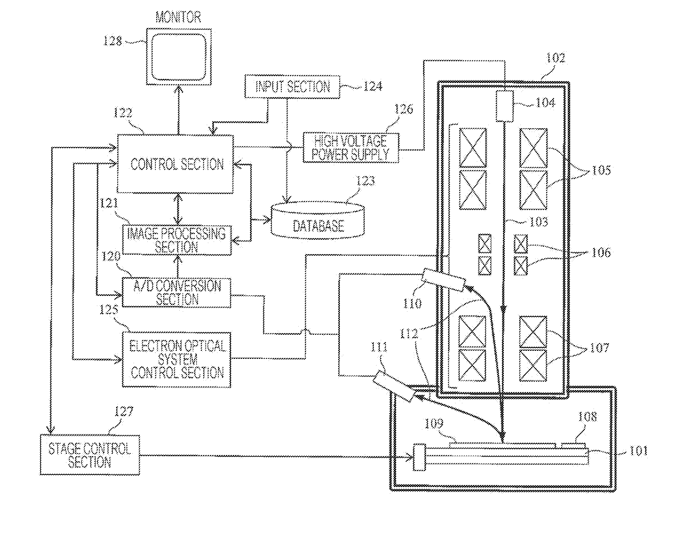
[0042]FIG. 1 is a diagram showing a scanning electron microscope according to the present invention. The scanning electron microscope includes a column 102 that is an electron optical system. The column 102 includes an electron source 104, a condenser lens 105, a deflection scanning coil 106, and an objective lens 107 that compose an electron optical system, the electron optical system irradiating an object with an electron beam 103. In addition, the scanning electron microscope includes detectors 110 and 111. The detectors are not limited to the detectors 110 and 111.
[0043]The electron source 104 is composed of an electron gun having a cathode (not shown) that is kept at a negative high potential and an anode (not shown) disposed at an exit of an electron beam. In the electron source 104, a voltage applied between the cathode and anode of the electron gun can be changed. When the voltage of the electron source 104, referred to as an acceleration voltage, is changed, the electron so...
second embodiment
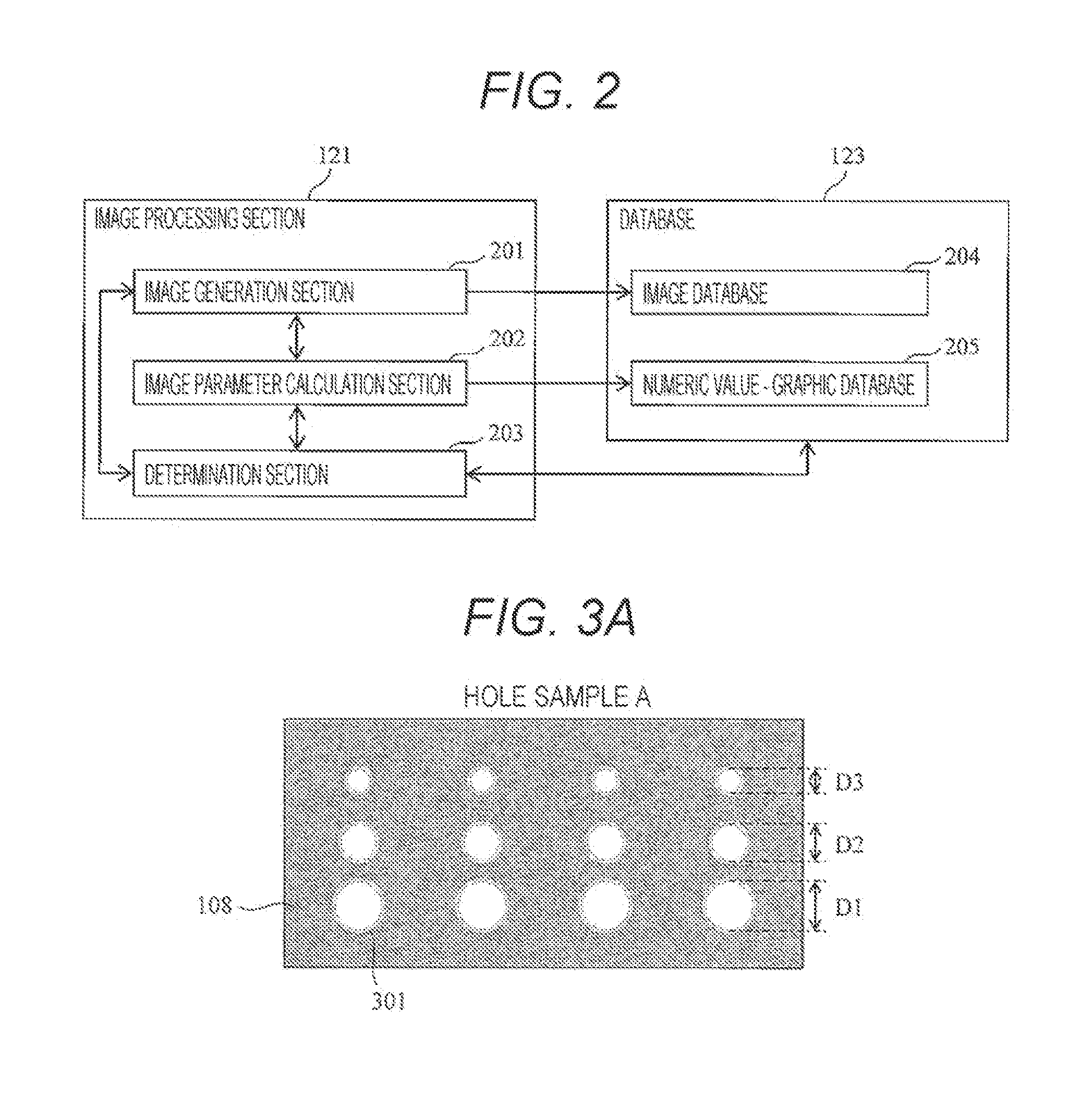
[0097]Next, a structure that has an image processing section 121 and a database 123 and that optimizes etching time (treatment conditions) will be described. FIG. 9A and FIG. 9B show an example of an reference sample 108 that is used in the present embodiment. According to the present embodiment, a hole sample B imitates a structure of a three-dimensional laminate device. The hole sample B has a plurality of holes whose diameter is the same. The hole sample B is etched for different etching times so that holes having different depths are formed.
[0098]According to the present embodiment, with the hole sample B as the reference sample 108, data that is stored in an image database 204 and a numeric value-graphic database 205 in the database 123 is created. A process for generating a graph from the reference sample 108 is the same as that shown in FIG. 6.
[0099]FIG. 9A is an SEM image of the hole sample B. FIG. 9B is a diagram showing a cross-sectional structure of the hole sample B. The...
third embodiment
[0109]Next, an embodiment in which an SEM measurement instrument, having a pattern size measurement function is provided with an image processing section 121 and a database 123 will be described. FIG. 11 is a flow chart showing an inspection process implemented by the SEM measurement instrument.
[0110]First, parameters are input through an input section 124. As described above, the parameters are sample information, coordinate information of image acquisition positions of a sample, coordinate information and range information of pattern portions and their neighboring portions necessary for acquiring brightness ratios, and the like. According to the present embodiment, parameters for a sample 109 that is a wafer sample that has been etched are input. In addition, imaging conditions for an SEM (conditions such as acceleration voltage) are input through the input section 124. Thereafter, the following process is implemented.
[0111]Next, the sample 109 is loaded on a sample stage 101 (at ...
PUM
 Abstract
Description
Claims
Application Information
 - R&D Engineer
- R&D Manager
- IP Professional
- Industry Leading Data Capabilities
- Powerful AI technology
- Patent DNA Extraction
Browse by: Latest US Patents, China's latest patents, Technical Efficacy Thesaurus, Application Domain, Technology Topic.
© 2024 PatSnap. All rights reserved.Legal|Privacy policy|Modern Slavery Act Transparency Statement|Sitemap