Optical element, and display device, electronic apparatus, lighting device using the same
- Summary
- Abstract
- Description
- Claims
- Application Information
AI Technical Summary
Benefits of technology
Problems solved by technology
Method used
Image

Examples
first exemplary embodiment
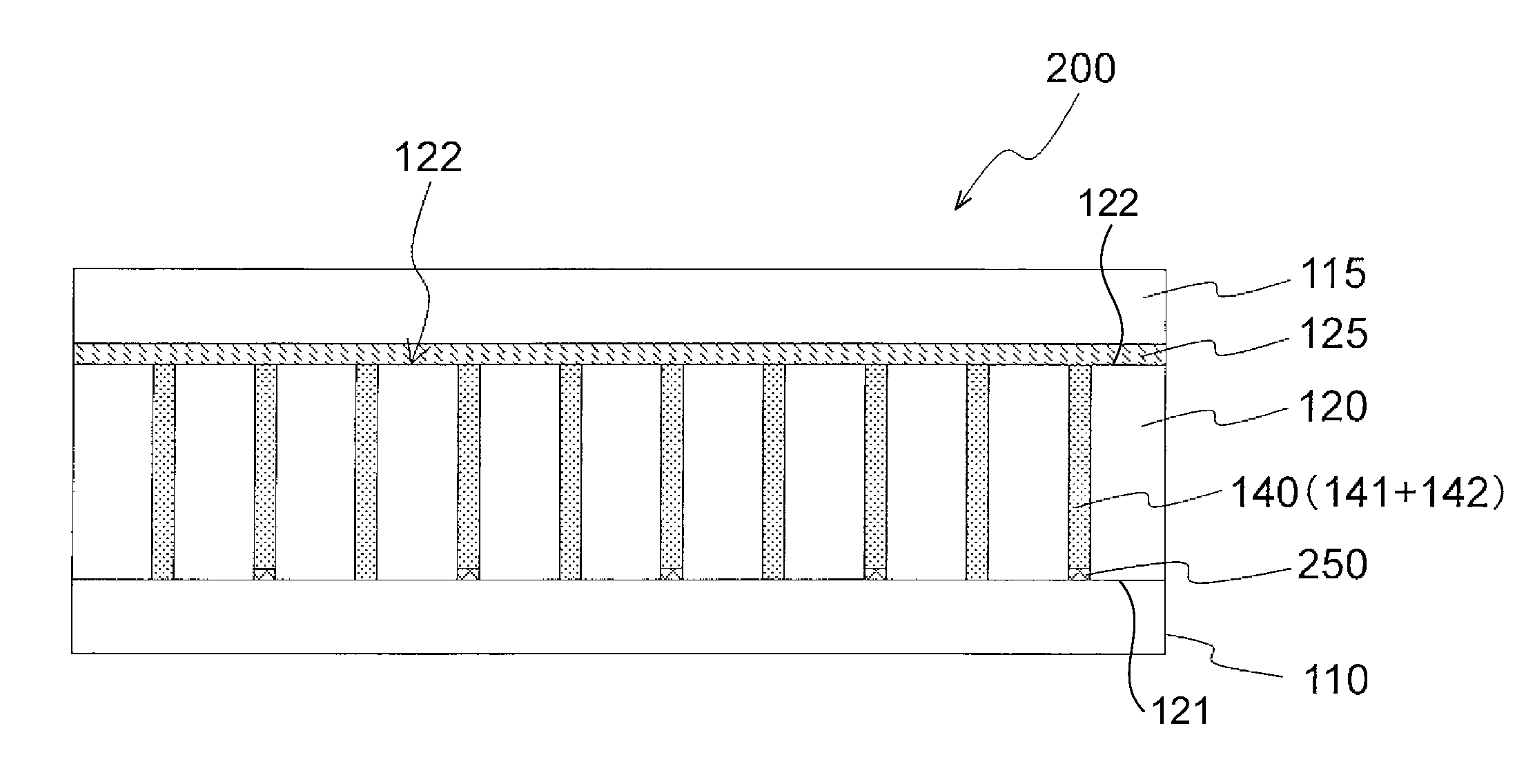
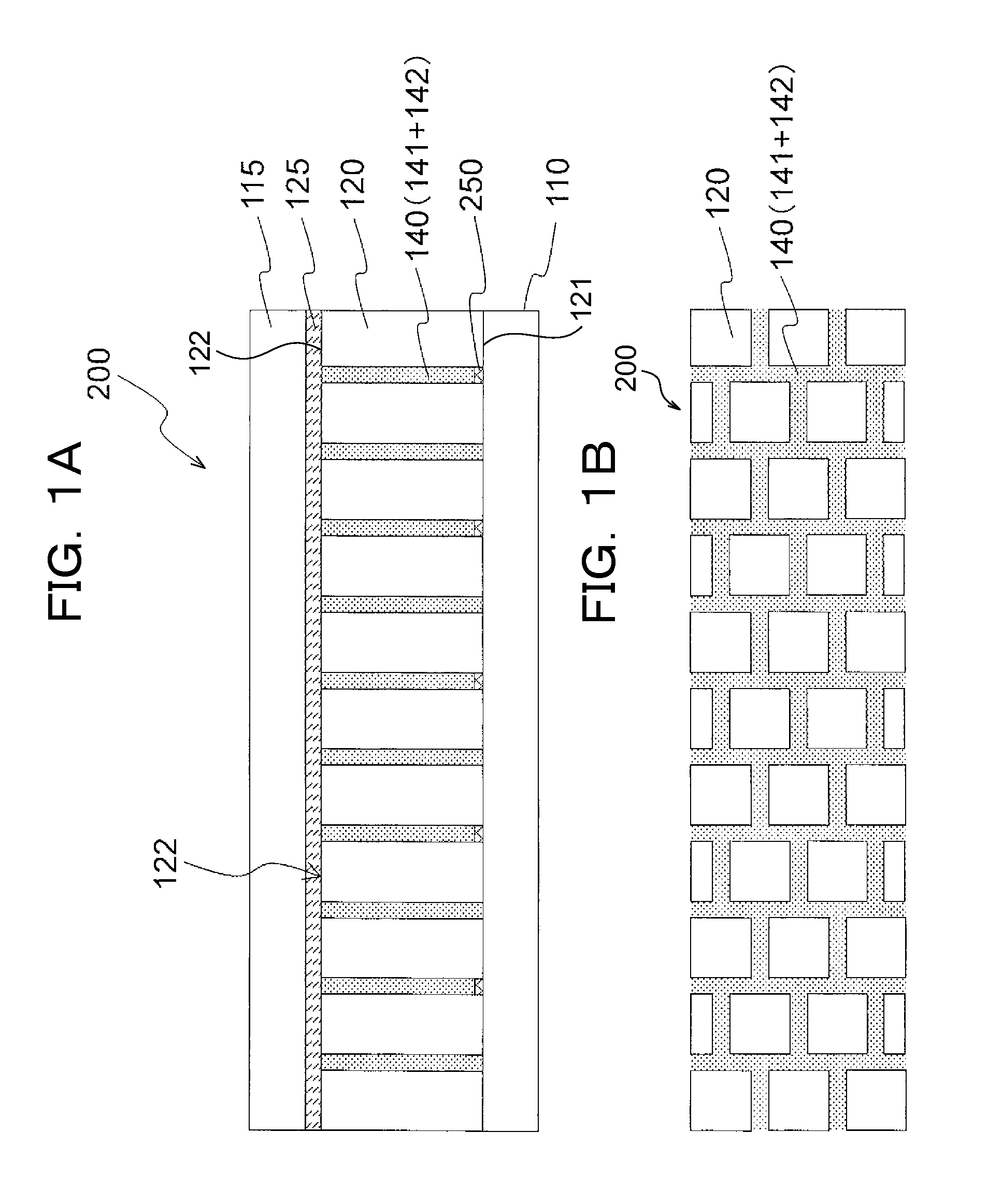
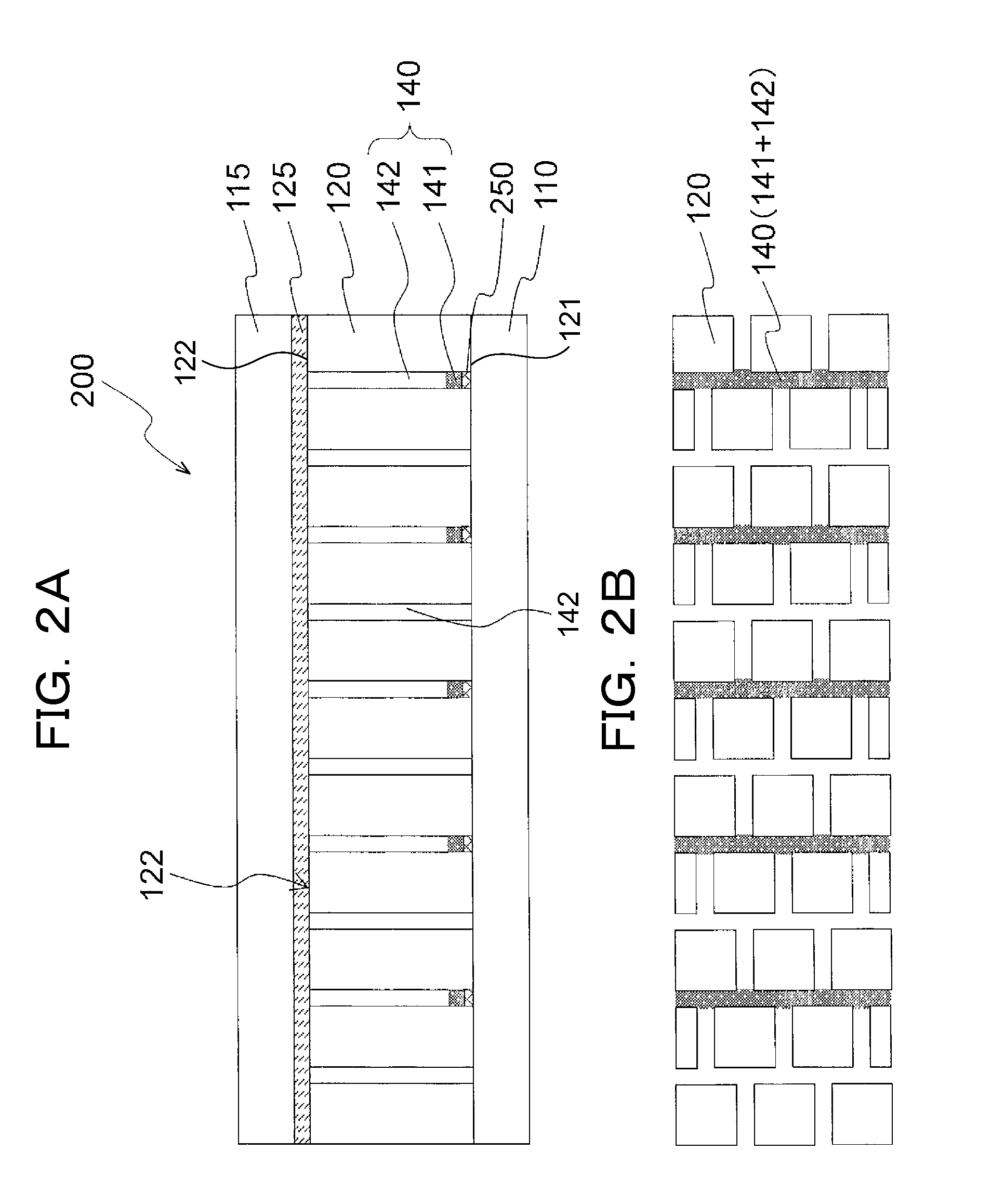
[0053]FIGS. 1A and 1B show illustrations of an optical element 200 of a first exemplary embodiment in a narrow viewing field mode, in which FIG. 1A is a longitudinal sectional view showing the optical element 200 that is cut in a face orthogonal to the display face of the optical element 200 and FIG. 1B is a surface view showing the display face from the normal direction. Further, FIGS. 2A and 2B show illustrations of the optical element 200 of the first exemplary embodiment in a wide viewing field mode, in which FIG. 2A is a longitudinal sectional view showing the optical element 200 that is cut in a face orthogonal to the display face of the optical element 200 and FIG. 2B is a surface view showing the display face from the normal direction. The details of the optical element according to the first exemplary embodiment will be described hereinafter.
[0054]The optical element 200 of the first exemplary embodiment includes: a first transparent substrate 110; a second transparent subs...
second exemplary embodiment
[0095]FIGS. 6A and 6B show longitudinal sectional views of an optical element 300 according to a second exemplary embodiment, in which FIG. 6A shows the state of the optical element 300 in a narrow viewing field mode and FIG. 6B shows a state of the optical element 300 in a wide viewing field mode. In FIGS. 6A and 6B, same reference numerals are applied to the elements same as those of FIGS. 1A and 1B. Hereinafter, details of the optical element 300 according to the second exemplary embodiment will be described.
[0096]As shown in FIG. 6A, in the second exemplary embodiment, a protection cover film 130 for covering the conductive patterns 250 is disposed between the transparent substrate 110 where the conductive patterns 250 are disposed and the light transmission regions 120.
The film thickness of the protection cover film 130 is appropriate to fall within a range of 10 nm to 1000 nm, and it is 300 nm in the second exemplary embodiment. As the structural material used for the protecti...
third exemplary embodiment
[0098]FIGS. 7A and 7B show longitudinal sectional views of an optical element 400 according to a third exemplary embodiment, in which FIG. 7A shows the state of the optical element 400 in a narrow viewing field mode and FIG. 7B shows a state of the optical element 400 in a wide viewing field mode. In FIGS. 7A and 7B, same reference numerals are applied to the elements same as those of FIGS. 1A and 1B.
Hereinafter, details of the optical element 400 according to the third exemplary embodiment will be described.
[0099]As shown in FIGS. 7A and 7B, in the third exemplary embodiment, the conductive patterns 250, the protection cover film 130, and the light transmission regions 120 are formed on the transparent substrate 110 as in the case of the second exemplary embodiment. On the top face of the light transmission regions 120, another transparent substrate 115 including a second protection cover film 135 for covering the transparent conductive film 125 stacked on the surface thereof is di...
PUM
 Abstract
Description
Claims
Application Information
 - R&D
- Intellectual Property
- Life Sciences
- Materials
- Tech Scout
- Unparalleled Data Quality
- Higher Quality Content
- 60% Fewer Hallucinations
Browse by: Latest US Patents, China's latest patents, Technical Efficacy Thesaurus, Application Domain, Technology Topic, Popular Technical Reports.
© 2025 PatSnap. All rights reserved.Legal|Privacy policy|Modern Slavery Act Transparency Statement|Sitemap|About US| Contact US: help@patsnap.com