Touch panel substrate and electronic apparatus
a technology of electronic equipment and substrate, applied in the field of touch panel substrate and electronic equipment, can solve problems such as the decrease of detection sensitivity, and achieve the effect of more even transmittance of the display surfa
- Summary
- Abstract
- Description
- Claims
- Application Information
AI Technical Summary
Benefits of technology
Problems solved by technology
Method used
Image

Examples
embodiment 1
[0037]Below, embodiments of the present invention are described in detail using FIGS. 1 to 10.
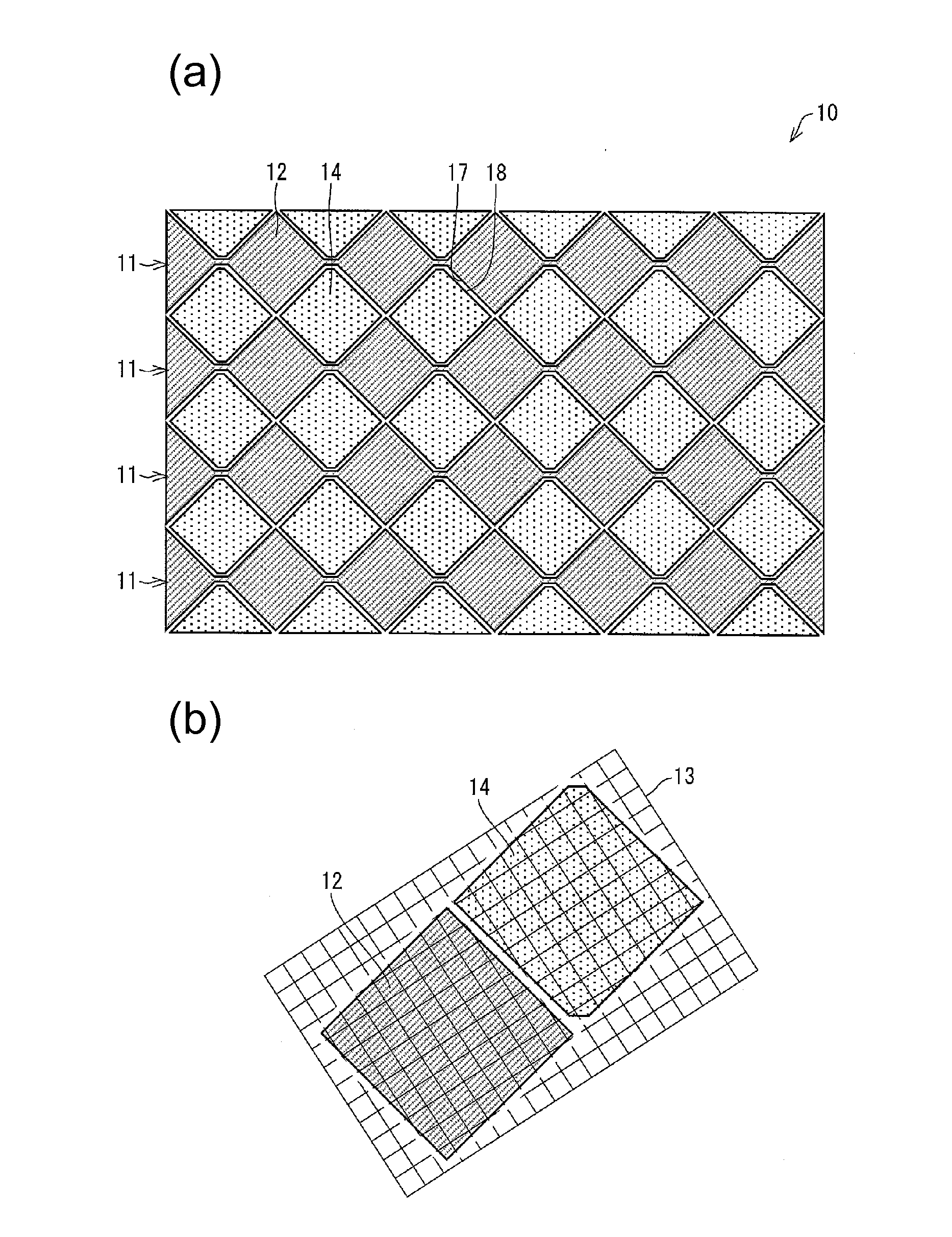
[0038]FIG. 1 is a cross-sectional view of an electronic apparatus 1 according to the present embodiment. As shown in FIG. 1, the electronic apparatus 1 includes a touch panel substrate 2 and a display device 3.
[0039]Various display devices such as a liquid crystal display device or an organic EL display device can be used for the display device 3. The display device 3 includes a display panel 4 and a backlight 5 disposed on the back side of the display panel 4 (the surface opposite to the display surface) and emits light toward the display panel 4. In addition, the display device 3 includes various driver circuits (not shown) that control an image displayed on the display surface of the display panel 4.
[0040]
[0041]The touch panel substrate 2 is a capacitive touch panel substrate disposed on the display surface side of the display panel 4. The touch panel substrate 2 is configured by layerin...
embodiment 2
[0091]Another embodiment according to the present invention is described below with reference to FIGS. 11 to 12. For ease of explanation, the components having the same functions as those in the drawings described in the embodiment above are given the same reference characters, and the descriptions thereof are omitted.
[0092]
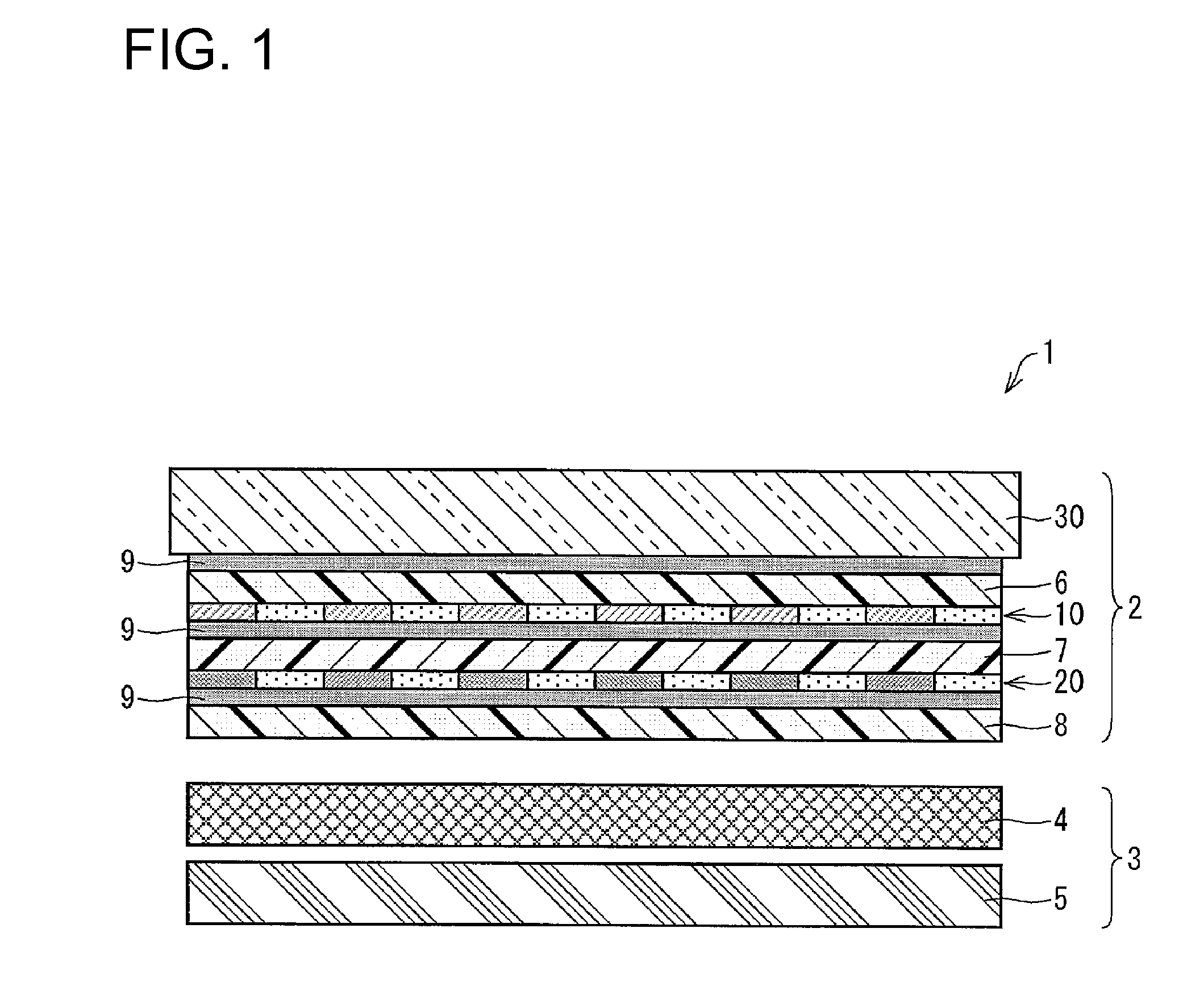
[0093]FIG. 11 is a plan view showing a first electrode layer of a touch panel substrate according to the present embodiment, FIG. 11(a) is a view showing cuts in first conductive lines of a first electrode layer, and FIG. 11(b) is an enlarged view of a dummy electrode shown in FIG. 11(a). FIG. 12 is a plan view showing a detailed configuration of first conductive lines of a touch panel substrate according to the present embodiment.
[0094]As shown in FIG. 11(a), second cuts 116 are provided in a first electrode layer 110 of a touch panel substrate according to the present embodiment. The second cuts 116 sever first conductive lines 13 that constitute first sensor e...
embodiment 3
[0100]Another embodiment according to the present invention is as described below with reference to FIGS. 13 to 16. For ease of explanation, the components having the same functions as those in the drawings described in the embodiment above are given the same reference characters, and the descriptions thereof are omitted.
[0101]
[0102]Below, the configuration of a first electrode layer 210 and a second electrode layer 220 of a touch panel substrate according to the present embodiment is described specifically.
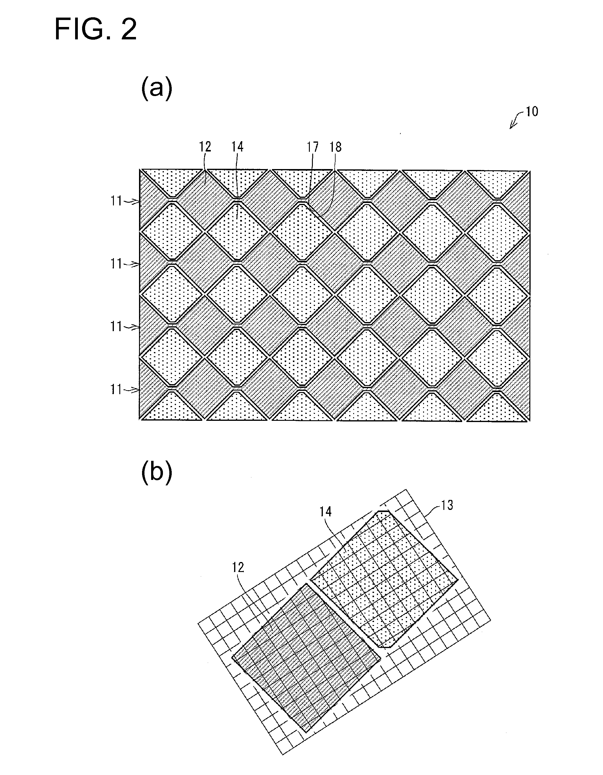
[0103]FIG. 13 is a plan view showing a configuration of a first electrode layer of a touch panel substrate according to the present embodiment, FIG. 13(a) is a view showing a configuration of first sensor electrodes, and FIG. 13(b) is a view showing a configuration of first conductive lines.
[0104]FIG. 14 is a plan view showing a configuration of a second electrode layer of a touch panel substrate according to the present embodiment, FIG. 14(a) is a view showing a configuration of...
PUM
 Abstract
Description
Claims
Application Information
 - R&D
- Intellectual Property
- Life Sciences
- Materials
- Tech Scout
- Unparalleled Data Quality
- Higher Quality Content
- 60% Fewer Hallucinations
Browse by: Latest US Patents, China's latest patents, Technical Efficacy Thesaurus, Application Domain, Technology Topic, Popular Technical Reports.
© 2025 PatSnap. All rights reserved.Legal|Privacy policy|Modern Slavery Act Transparency Statement|Sitemap|About US| Contact US: help@patsnap.com