
Display panel and manufacturing method thereof, and display apparatus

A display panel, consistent technology, applied in optics, instruments, electrical components, etc., can solve the problems affecting the display effect of the screen, and achieve the effect of improving the twill Mura phenomenon, uniform light transmittance, and improving the display effect.

Inactive Publication Date: 2017-05-31
BOE TECH GRP CO LTD +1
View PDF4 Cites 2 Cited by
  • Summary
  • Abstract
  • Description
  • Claims
  • Application Information

AI Technical Summary

Problems solved by technology

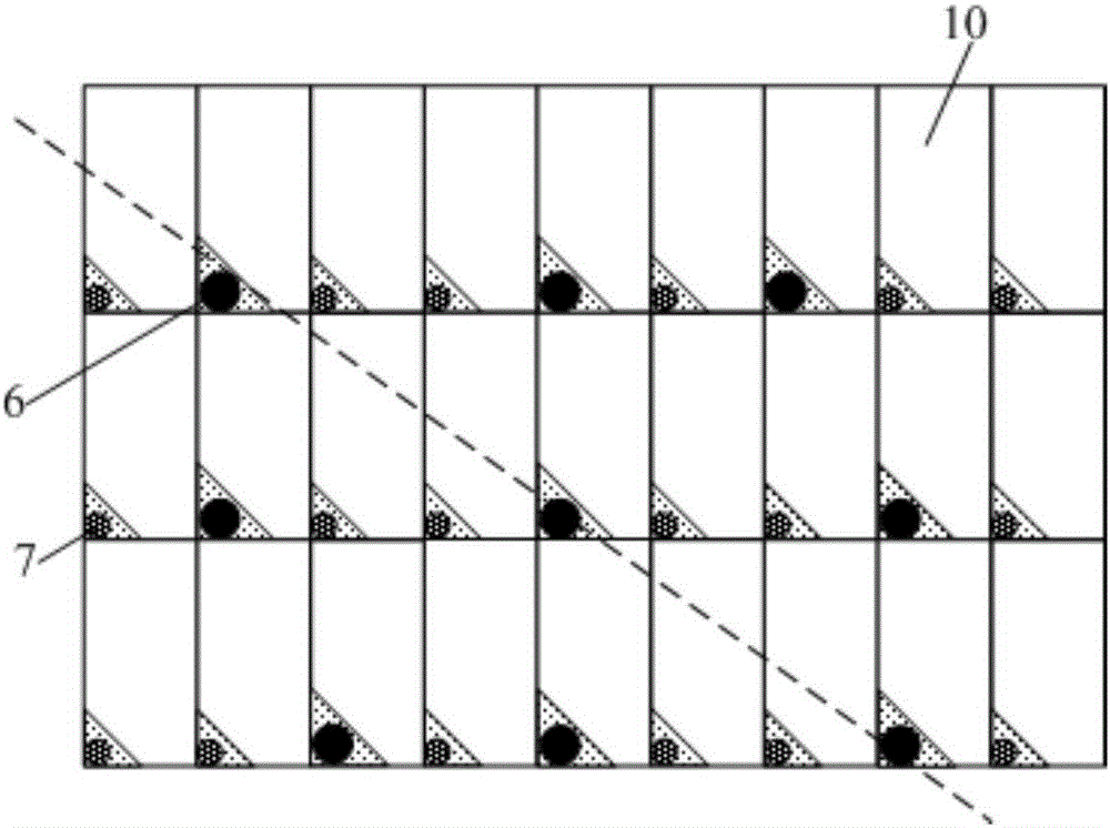
[0004] like figure 1 As shown, the main spacers 6 are usually evenly distributed inside the display panel, which is a typical design occupancy diagram of the density of the main spacers 6 being 1 / 18. When viewed from the entire field of view, all the main spacers 6 are located Because the brightness of the pixel area 10 is lower than that of all the pixel areas 10 where the auxiliary spacers 7 are located, a series of oblique shadows (Mura) will be formed, thereby affecting the display effect of the picture.

Method used


Image

  • Display panel and manufacturing method thereof, and display apparatus
  • Display panel and manufacturing method thereof, and display apparatus
  • Display panel and manufacturing method thereof, and display apparatus

Examples


Embodiment 1

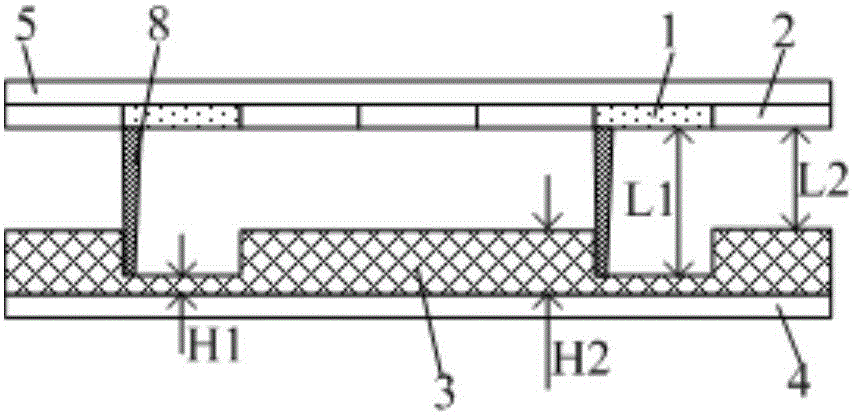
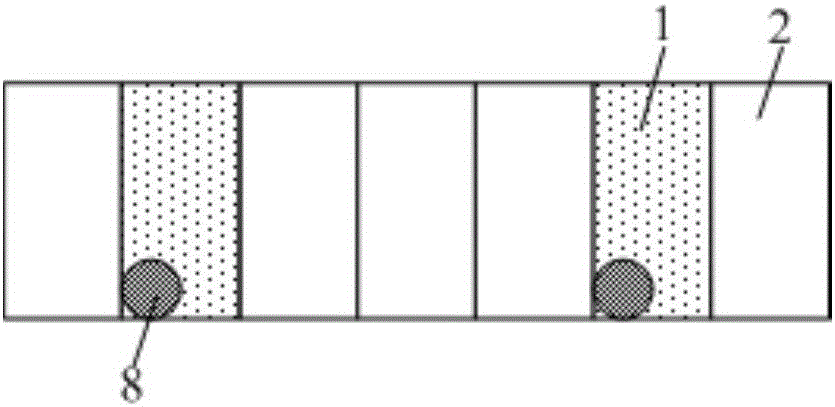
[0042] This embodiment provides a display panel, such as figure 2 and image 3 As shown, the display panel includes a first sub-pixel region 1 and a second sub-pixel region 2, the aperture ratio of the first sub-pixel region 1 is smaller than the aperture ratio of the second sub-pixel region 2; the display panel also includes an insulating layer 3, the insulating layer The thickness H1 corresponding to the first sub-pixel area 1 of 3 is smaller than the thickness H2 corresponding to the second sub-pixel area 2, so that the cell gap L1 corresponding to the first sub-pixel area 1 of the display panel is larger than the corresponding second sub-pixel area 2 The cell gap L2, so that the aperture ratios of the first sub-pixel area 1 and the second sub-pixel area 2 are uniform.

[0043] Wherein, the display panel refers to a liquid crystal display panel. Since the cell thickness of the display panel is positively correlated with its liquid crystal light effect during display, that ...

Embodiment 2

[0056] This embodiment provides a display panel, such as Figure 4 and Figure 5 As shown, the display panel includes a first sub-pixel region 1 and a second sub-pixel region 2, the aperture ratio of the first sub-pixel region 1 is smaller than the aperture ratio of the second sub-pixel region 2; the display panel also includes an insulating layer 3, the insulating layer The thickness H1 corresponding to the first sub-pixel area 1 of 3 is smaller than the thickness H2 corresponding to the second sub-pixel area 2, so that the cell gap L1 corresponding to the first sub-pixel area 1 of the display panel is larger than the corresponding second sub-pixel area 2 The cell gap L2, so that the aperture ratios of the first sub-pixel area 1 and the second sub-pixel area 2 are uniform.

[0057] Wherein, the display panel refers to a liquid crystal display panel. Since the cell thickness of the display panel is positively correlated with its liquid crystal light effect during display, th...

Embodiment 3

[0070] This embodiment provides a display panel, which is different from Embodiment 1-2, such as Figure 6 and Figure 7 As shown, on the basis of the display panel provided in Embodiment 2, the display panel further includes a third sub-pixel region 9, and the aperture ratio of the second sub-pixel region 2 is smaller than the aperture ratio of the third sub-pixel region 9; The third sub-pixel region 9 is not provided with any spacers; the thickness H2 of the insulating layer 3 corresponding to the second sub-pixel region 2 is smaller than the thickness H3 corresponding to the third sub-pixel region 9, so that the corresponding second sub-pixel of the display panel The cell gap L2 of the region 2 is larger than the cell gap L3 of the corresponding third sub-pixel region 9 , so that the aperture ratios of the second sub-pixel region 2 and the third sub-pixel region 9 are uniform.

[0071] Since the main spacer 6 correspondingly occupies a part of the area in the first sub-pix...


PUM


Abstract

The invention provides a display panel and a manufacturing method thereof, and a display apparatus. The display panel includes first sub pixel areas and second sub pixel areas, wherein the aperture ratio of the first sub pixel areas is less than that of the second sub pixel areas; the thickness of an insulation layer corresponding to the first sub pixel areas is less than the thickness of the insulation layer corresponding to the second sub pixel areas such that the cell gap of the display panel corresponding to the first sub pixel areas is greater than the cell gap of the display panel corresponding to the second sub pixel areas, and the aperture ratios of the first sub pixel areas and the second sub pixel areas are even. Liquid crystal lighting effect difference between the display panel corresponding to the first sub pixel areas and the display panel corresponding to the second sub pixel areas can remedy aperture ratio difference between the first sub pixel areas and the second sub pixel areas, and then the light transmittance of the display pane in the first sub pixel areas and the second sub pixel areas can be improved, the light transmittance of the display panel is more even, and the display effect of the display panel is improved.

Description

technical field [0001] The present invention relates to the field of display technology, in particular, to a display panel, a manufacturing method thereof, and a display device. Background technique [0002] Thin film transistor liquid crystal display (TFT-LCD) has the advantages of small size, low power consumption, and no radiation. It has developed rapidly in recent years and has occupied the mainstream position in the market. TFT-LCD is a precise and complex device composed of many components, mainly composed of color filter glass (Color Filter Glass, referred to as CF substrate), array substrate (TFT Glass, referred to as TFT substrate) and liquid crystal between the two substrates. When forming a box, the liquid crystal is poured on one of the substrates, and the sealing glue (which is mixed with a certain proportion of silicon balls of the calculated size) is coated on the other substrate, and finally through vacuum bonding and sealing glue. Curing forms a liquid cry...

Claims


Application Information

Patent Timeline
Patent Type & Authority Applications(China)
IPC IPC(8): G02F1/1339
CPCG02F1/13394G02F2201/40G02F1/133371G02F1/13396G02F1/136236H01L27/1248G02F1/133514G02F1/1368G02F1/133357
Inventor 朱锦明王辉刘佳郭远辉
Owner BOE TECH GRP CO LTD
Learn More