Capacitive touch pad

a capacitance touch and capacitance technology, applied in the direction of instruments, pulse techniques, keyboard-like device coding, etc., can solve the problems of achieve the effect of improving the capacitance touching panel, improving the flatness of the capacitance sensing structure, and avoiding uneven light deflection at different areas

Inactive Publication Date: 2014-03-18
YOUNG FAST OPTOELECTRONICS
View PDF6 Cites 2 Cited by
  • Summary
  • Abstract
  • Description
  • Claims
  • Application Information

AI Technical Summary

Benefits of technology

[0004]Thereby, the object of the present invention is to provide an improved capacitance touching panel. Precise etching lines are formed on a transparent conductive film so as to form with a desired pattern. As a result, the hollowed portion on the conductive film is reduced greatly and thus the flatness of the capacitance sensing structure will be improved and the transmittances in different areas will tend to be uniform. Thus the image distortion in the screen below the touch panel is improved. Besides, the etching lines divide the waste etching areas on the conductive lines into a plurality of small units which can reduce the capacitances of the noises.

Problems solved by technology

However, the areas having the capacitance sensing area and the etched portions (namely, the hollowed portions of the conductive films) have different light transmittances so that the light deflections at different areas are not uniform.

Method used


Image

  • Capacitive touch pad
  • Capacitive touch pad
  • Capacitive touch pad

Examples


Embodiment Construction

[0018]In order that those skilled in the art can further understand the present invention, a description will be provided in the following in details. However, these descriptions and the appended drawings are only used to cause those skilled in the art to understand the objects, features, and characteristics of the present invention, but not to be used to confine the scope and spirit of the present invention defined in the appended claims.

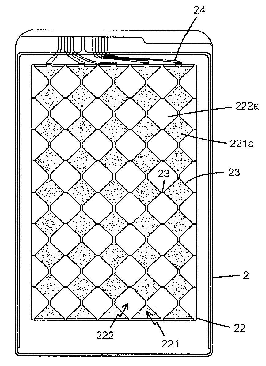
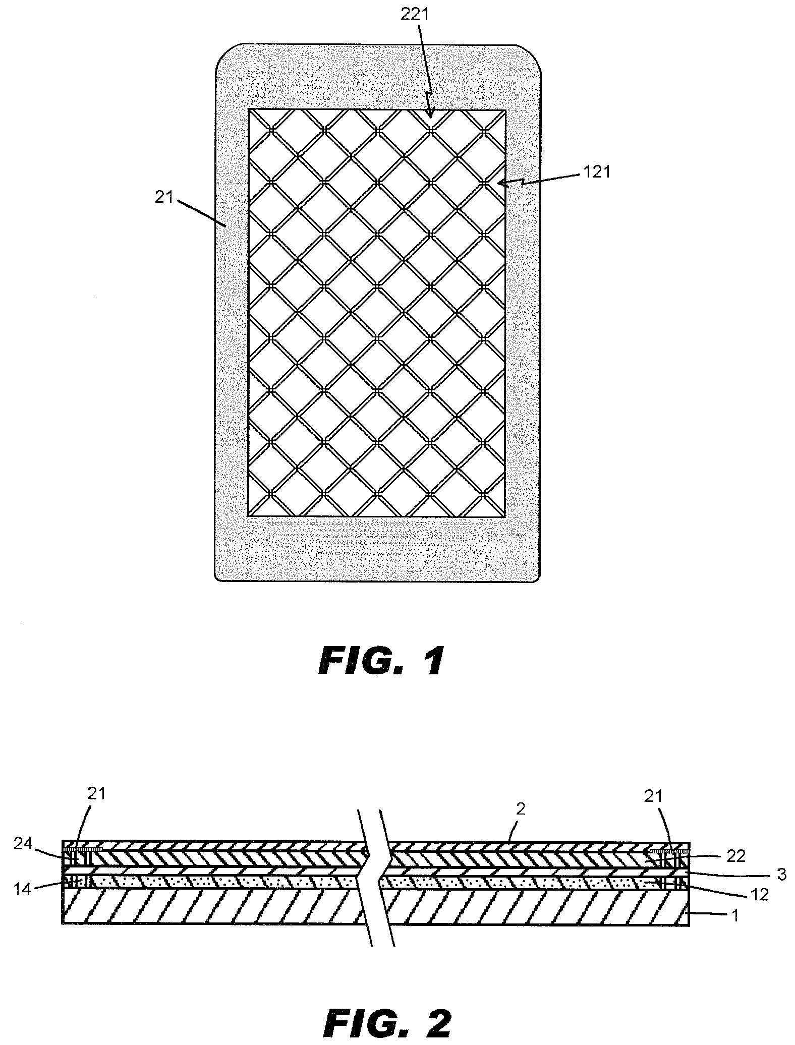
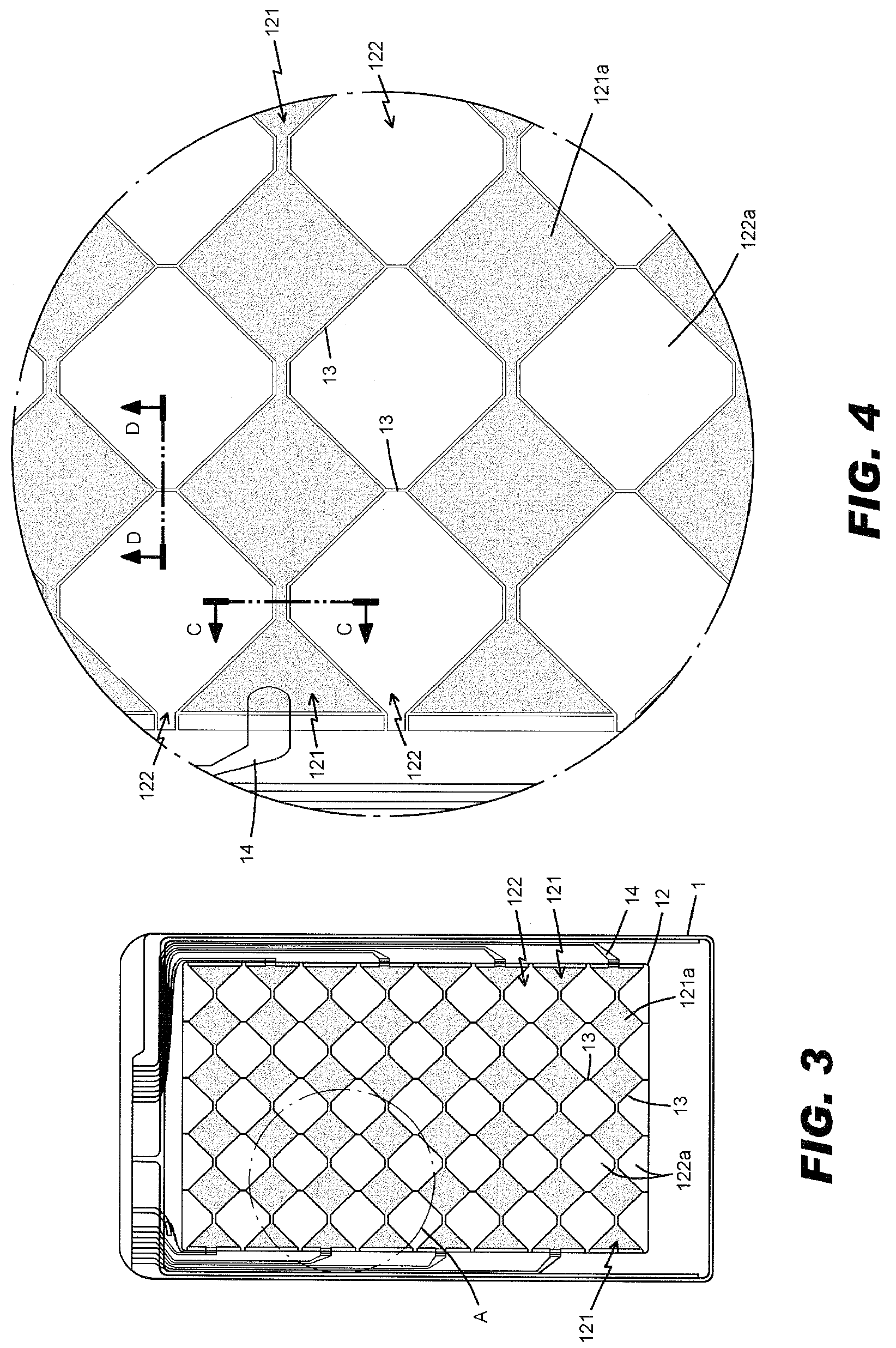
[0019]With reference to FIGS. 1 and 2, a preferred embodiment of the present invention is illustrated. The capacitive touch sensor of the present invention includes a lower substrate 1 and an upper panel 2. Each upper surface of the lower substrate 1 and the upper panel 2 is installed with a capacitive sensing layer 12, 22. A gluing combining layer 3 is installed between the lower capacitive sensing layer 12 and the upper capacitive sensing layer 22. Each of the lower substrate 1 and the upper panel 2 is made of highly transparent material and is a...


PUM


Abstract

A capacitive touch panel has precise etching lines formed on a transparent conductive film so as to form with a desired pattern. As a result, the hollowed portion on the conductive film will be reduced greatly and thus the flatness of the capacitance sensing structure will be improved and the transmittances in different areas will tend to be uniform. Thus the image distortion in the screen below the touch panel will be improved. Besides, the etching lines will divide the waste etching areas on the conductive lines into a plurality of small units which can reduce the capacitances of the noises.

Description

FIELD OF THE INVENTION[0001]The present invention related to a capacitive touch panel, in particular to a capacitive touch panel with uniform light transmittances and having lower noise capacitance.BACKGROUND OF THE INVENTION[0002]A capacitance touch panel will has capacitance effect by a touching to the panel. The variation of the capacitance is used to detect the touch position so as to achieve the object of signal input. The capacitance touch panel can be inputted by fingers so that the input operation is very convenient. No large pressure is applied to the panel and thus no damage will generate in the panel. Furthermore, the elements of the panel are less and yield rate is high so that it is suitable to mass production with less cost. Thus it is widely used in communication, computers and other consumer devices.[0003]In prior art capacitance touch panels, a plurality of X traces and Y traces are intersectedly arranged. The capacitive sensing units of the X traces and Y traces ar...

Claims


Application Information

Patent Timeline
Patent Type & Authority Patents(United States)
IPC IPC(8): H03K17/975
CPCG06F3/044H03K17/9622G06F3/0445
Inventor LIN, TEH-ZHENG
Owner YOUNG FAST OPTOELECTRONICS
Why Eureka
Try Eureka