Stack structure of high frequency printed circuit board

Active Publication Date: 2016-03-24
KUANG YING COMPUTER EQUIP CO LTD
View PDF8 Cites 9 Cited by
  • Summary
  • Abstract
  • Description
  • Claims
  • Application Information

AI Technical Summary

Benefits of technology

[0004]The main object of the present invention is to provide a stack structure of a printed circuit board, solving the interference problem generated from high frequency signals effectively by collocating a transmission conductor pin group containing high frequency signals with structures such as through hole portions, trace portions and ground layers by means of pairs of signal terminals and pairs of power terminals arranged in a group of four.
[0005]To achieve the above object, the present invention mainly includes a transmission conductor pin group in a form of single row, first differential power unit, a second differential power unit configured at one side of the first differential power unit, a first differential detection unit configured at one side of the second differential power unit far away from the first differential power unit, a second differential detection unit configured at one side of the first differential detection unit far away from the second differential power unit, a third differential power unit configured at on

Problems solved by technology

Since interference intensity is inversely proportional to distance, the more delicate electronic products are, the easier they are failure because of interferences.
Signals with a frequency larger than 2.4 GHz are referred to as high frequency signals, the interference of which will decrease the sensitivity of wireless reception, and further reduces reception range, being

Method used


Image

  • Stack structure of high frequency printed circuit board
  • Stack structure of high frequency printed circuit board
  • Stack structure of high frequency printed circuit board

Examples


Embodiment Construction

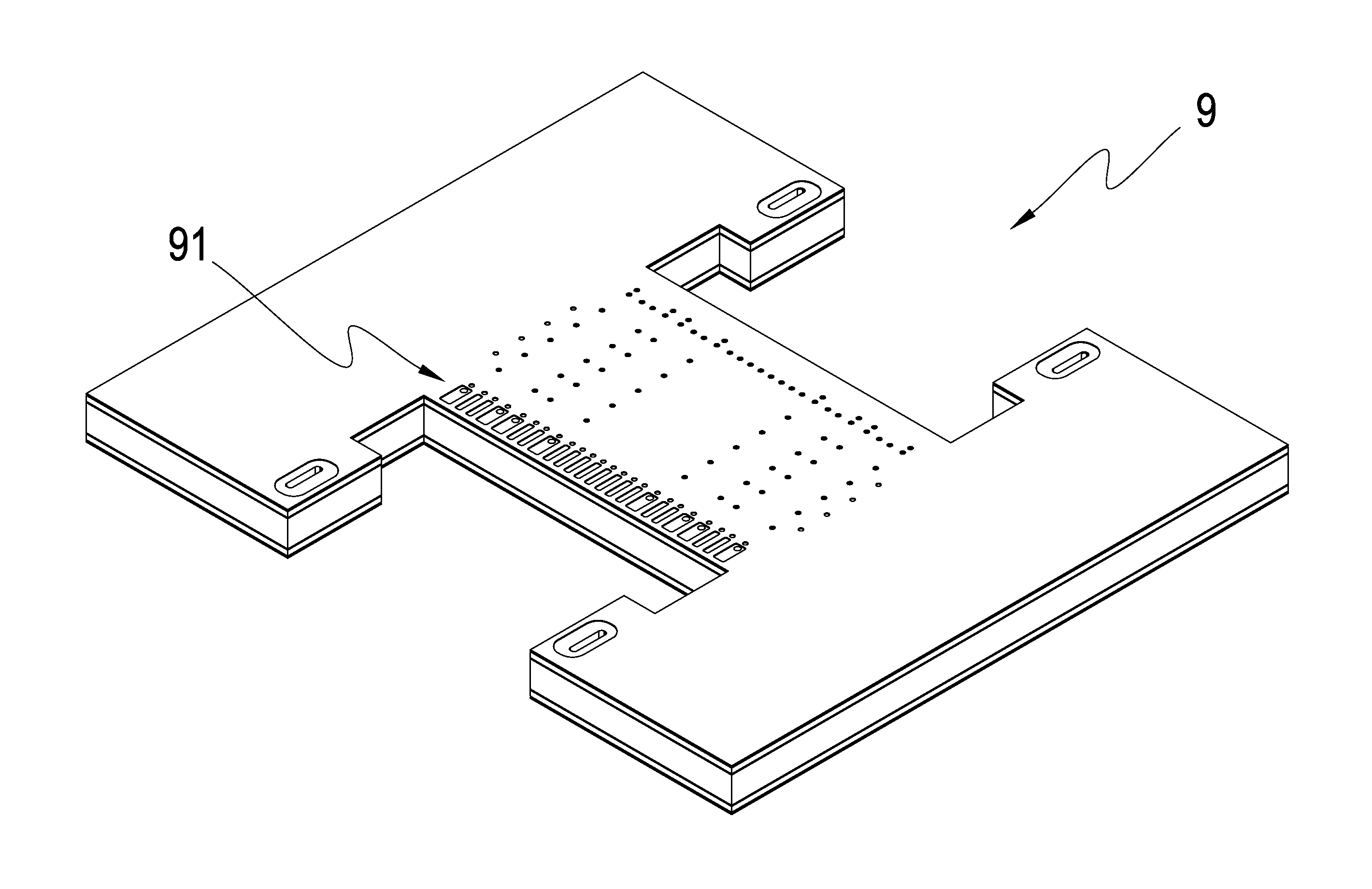
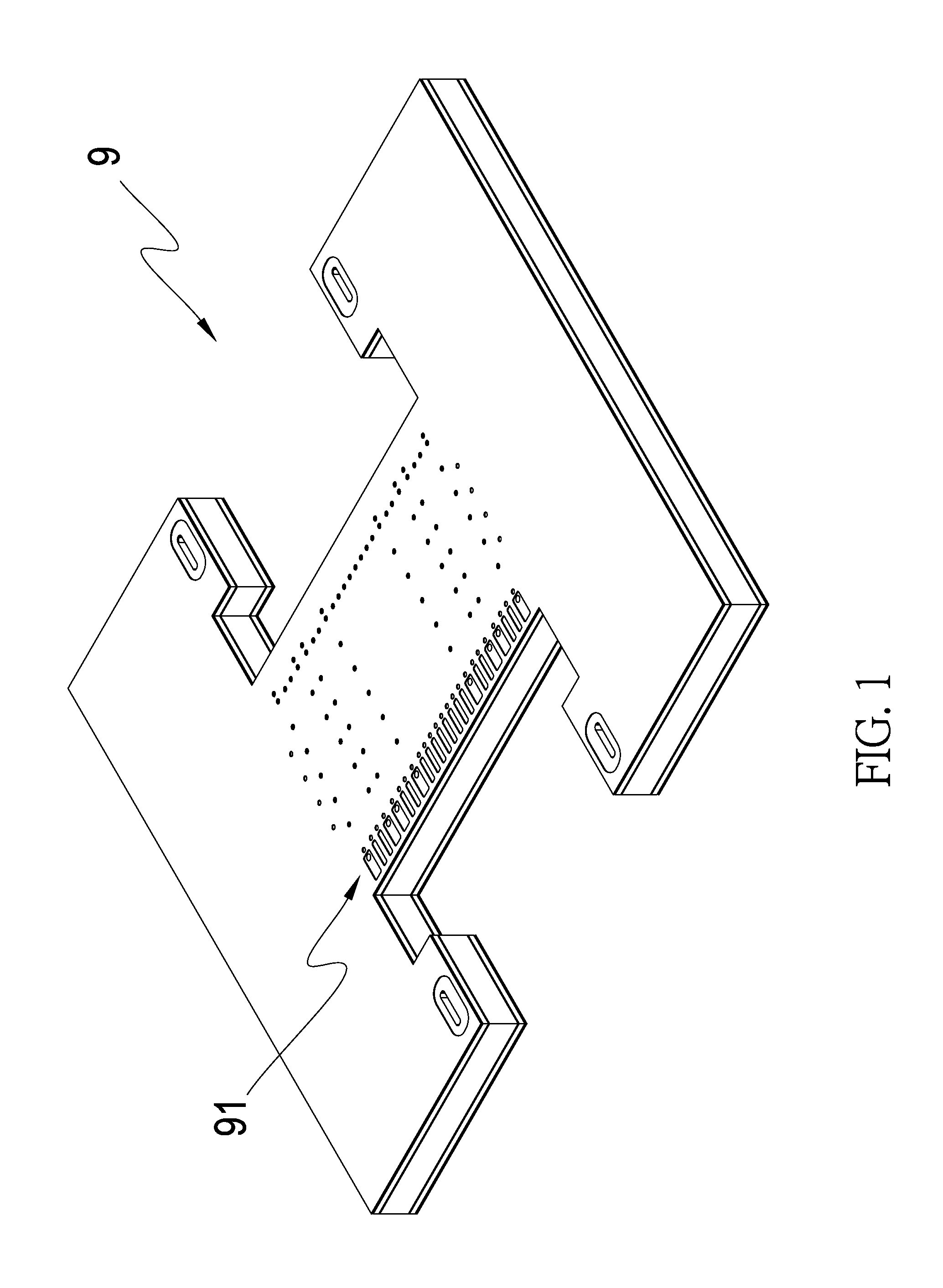
[0013]Referring to FIGS. 1 to 4, a high frequency printed circuit board 9 includes a single row form of transmission conductor pin group 91, and further mainly includes:

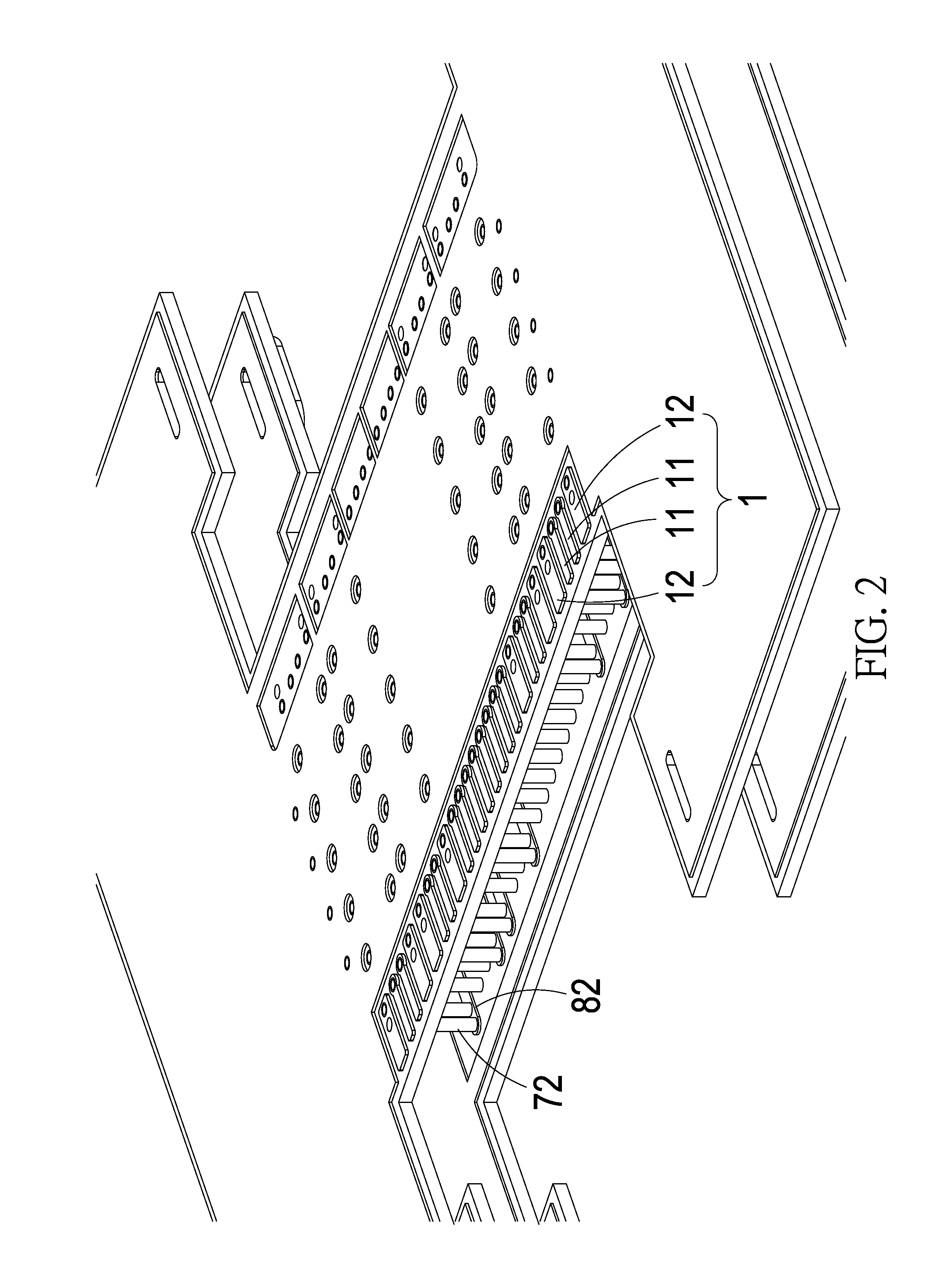
[0014]a first differential power unit 1, including a pair of first differential signals 11 and a pair of first power transmissions 12 respectively configured at the two sides of the pair of first differential signals 11;

[0015]a second differential power unit 2, configured at one side of the first differential power unit 1, and including a pair of second differential signals 21 and a pair of second power transmissions 22 respectively configured at the two sides of the pair of second differential signals 21;

[0016]a first differential detection unit 5, configured at one side of the second differential power unit 2 far away from the first differential power unit 1, and including a pair of fifth differential signals 51 and a pair of fifth detection signals 52 respectively configured at the two sides of the pair of fifth d...


PUM


Abstract

A stack structure of a high frequency printed circuit, mainly includes a transmission conductor pin group in a form of single row, where each signal pair and each transmission pair of the transmission conductor pin group respectively have a through hole portion thereon, and the inner layer of the circuit board has a trace portion in electric connection with the through hole portion, allowing each four terminals to be formed into one group. Utilizing the clever arrangement of the through hole portions and trace portions separates each terminal properly, thereby increasing the property of transmitted signals, and, at the same time, reducing noise interferences such as EMI and RFI.

Description

TECHNICAL FIELD OF THE INVENTION[0001]The present invention relates to a stack structure of a high frequency printed circuit board, capable of isolating high frequency signals effectively so as to decrease the electromagnetic interference and radio frequency interference caused from the high frequency signals to circuit boards or other external electronic products.DESCRIPTION OF THE PRIOR ART[0002]Since interference intensity is inversely proportional to distance, the more delicate electronic products are, the easier they are failure because of interferences. Therefore, how to solve interference problems is an urgent priority.[0003]Signals with a frequency larger than 2.4 GHz are referred to as high frequency signals, the interference of which will decrease the sensitivity of wireless reception, and further reduces reception range, being sufficient enough to influence the normal use of wireless devices; such signals cannot be eliminated through filtering such that external housings ...

Claims


Application Information

Patent Timeline
IPC IPC(8): H05K1/02H05K1/14
CPCH05K1/0224H05K2201/042H05K1/144H05K1/0219H05K1/0225H05K1/0245H05K1/117H05K2201/09336H05K2201/09718H05K2201/10189H05K2201/10446
Inventor CHUNG, HSUAN-HOTSENG, CHIEN-LING
Owner KUANG YING COMPUTER EQUIP CO LTD
Why Eureka
Try Eureka