Conductive pattern and electrode pattern of single-layer capacitive touchscreen

a capacitive touchscreen and conductive pattern technology, applied in the field of conductive pattern and electrode pattern of single-layer capacitive touchscreen, can solve the problems of increasing the electric resistance moire or other problems, and the light transmittance of the optically transparent conductive material utilizing an ito conductive film is unfavorably low, and achieves low light transmittance, hardly producing moire, and high light transmittance

Inactive Publication Date: 2016-03-31
MITSUBISHI PAPER MILLS LTD
View PDF21 Cites 26 Cited by
  • Summary
  • Abstract
  • Description
  • Claims
  • Application Information

AI Technical Summary

Benefits of technology

[0030]The present invention can provide a conductive pattern which has low visibility, has a high light transmittance, and hardly produces moire, and therefore is suitable as an optically transparent electrode for a capacitive touchscreen, and can provide an electrode pattern of a single-layer capacitive touchscreen.

Problems solved by technology

However, since an ITO conductive film has high refractive index and high surface light reflectivity, the light transmittance of an optically transparent conductive material utilizing an ITO conductive film is unfavorably low.
In addition, due to low flexibility, the ITO conductive film is prone to crack when bent, resulting in increased electric resistance of the optically transparent conductive material.
However, in cases where two layers OF the metal mesh film described in Patent Literature 1 to 7 are overlapped with each other, the respective mesh patterns interfere with each other, causing moire or other problems.
However, overlapping two metal mesh film layers results in a low light transmittance, leading to a dark touchscreen.

Method used


Image

  • Conductive pattern and electrode pattern of single-layer capacitive touchscreen
  • Conductive pattern and electrode pattern of single-layer capacitive touchscreen
  • Conductive pattern and electrode pattern of single-layer capacitive touchscreen

Examples


Embodiment Construction

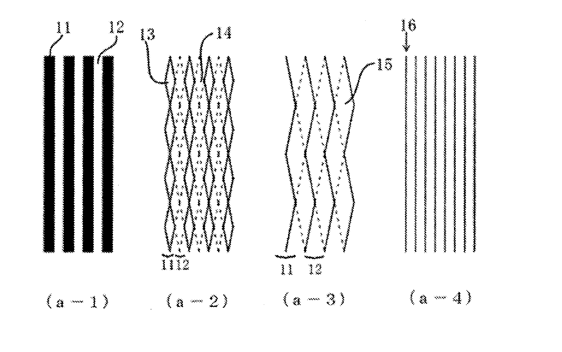
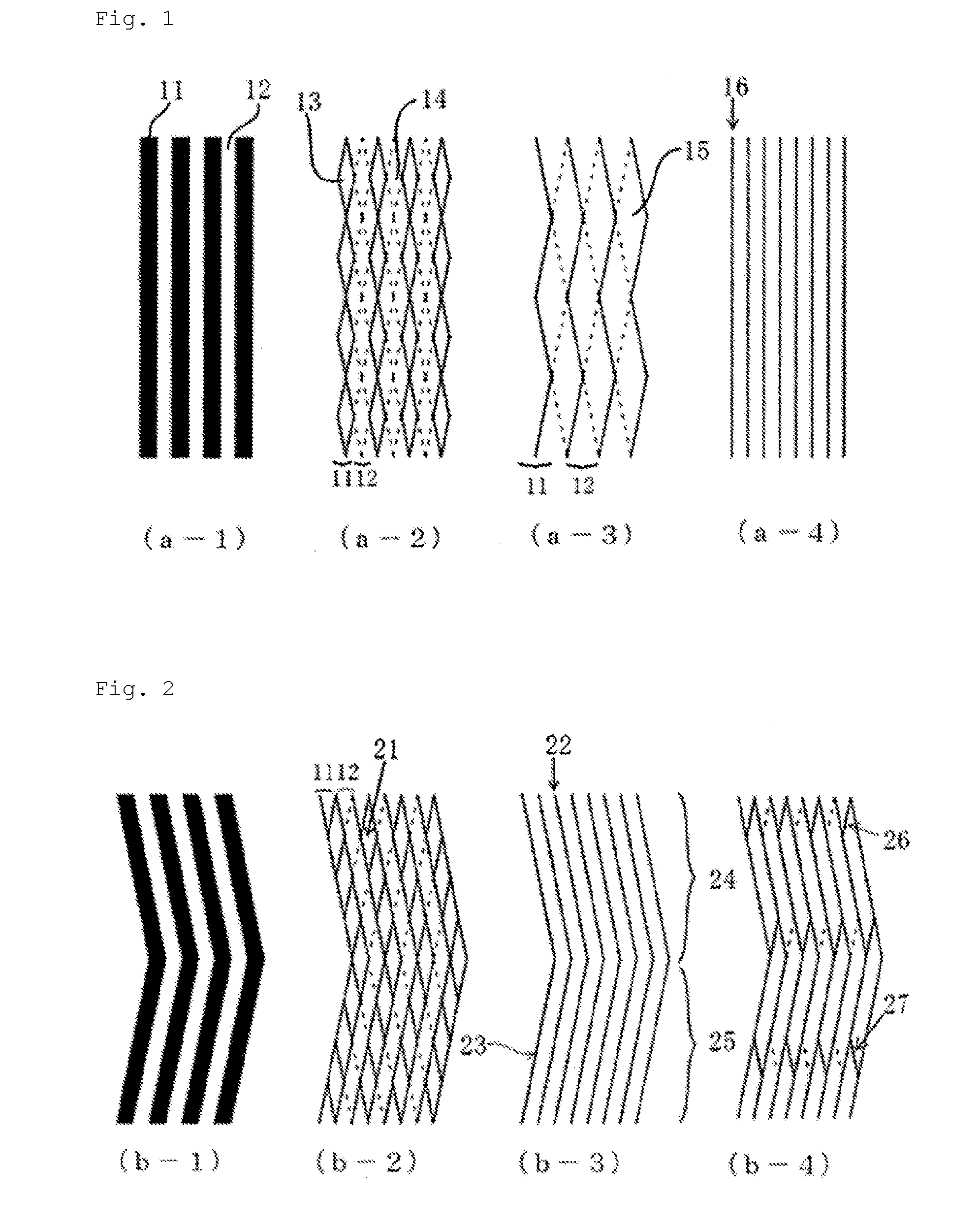
[0043]Hereinafter, the present invention will be illustrated in detail with reference to drawings, but it is needless to say that the present invention is not limited thereto and various alterations and modifications may be made without departing from the technical scope of the invention.

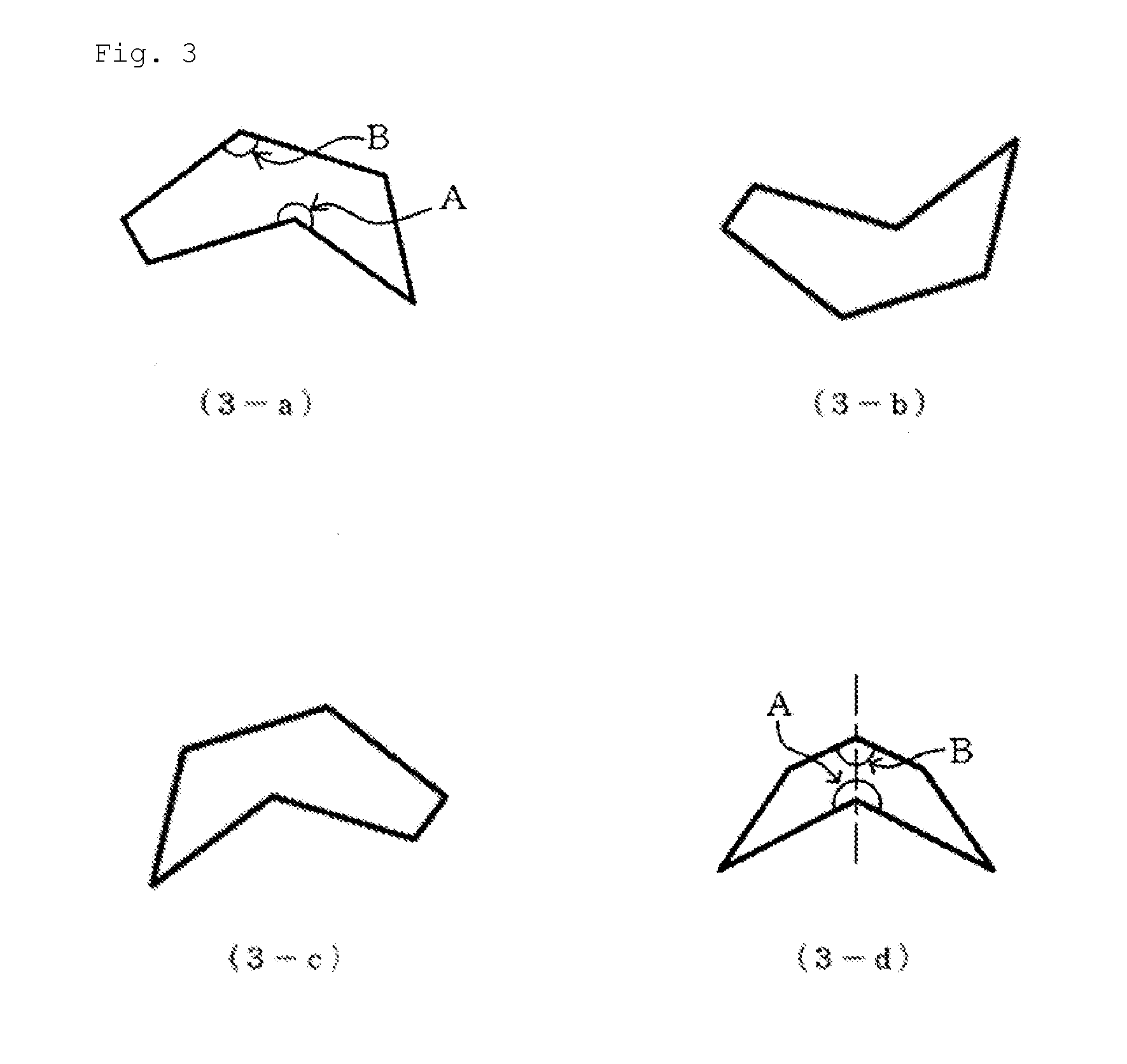
[0044]FIG. 3 illustrates unit graphics used for the conductive pattern of the present invention, and lines (excluding lines for explanation, arrows, and symbols) represent metal thin lines. The unit graphic of the present invention is a graphic being selected from a concave hexagon and the congruent figures thereof, the concave hexagon having one inner angle greater than 180° (Angle A) and five inner angles each smaller than 180° with the proviso that the total of Angle A and the third angle from Angle A (Angle B) is 360°. In (3-a) of FIG. 3, Angle A is greater than 180° and the other five angles are smaller than 180°. When an angle adjacent to Angle A is counted as the first angle and the third ang...


PUM


Abstract

Provided is a conductive pattern which has low visibility, has a high light transmittance, and hardly produces moire, and therefore is suitable as an optically transparent electrode for a capacitive touchscreen. The conductive pattern has a row of unit graphics formed of a conductive metal thin line or a metal thin line having line breaks, the unit graphic is selected from a concave hexagon and the congruent figures thereof, the concave hexagon has one inner angle greater than 180° (Angle A) and five inner angles each smaller than 180° with the proviso that the total of Angle A and the third angle from Angle A (Angle B) is 360°, the unit graphics adjoiningly line up in the row, and the row of the unit graphics extends in a direction of the bisector of an angle formed by the bisector of Angle A and the bisector of Angle B.

Description

TECHNICAL FIELD[0001]The present invention relates to a conductive pattern of a conductive material mainly used for a touchscreen and an electrode pattern of a single-layer capacitive touchscreen.BACKGROUND ART[0002]In electronic devices, such as PDAs (personal digital assistants), laptop computers, office automation equipment, medical equipment, and car navigation systems, touchscreens are widely used as their display screens that also serve as input means.[0003]There are a variety of touch screens that utilize different position detection technologies, such as optical, ultrasonic, surface capacitive, projected capacitive, and resistive technologies. A resistive touchscreen has a configuration in which, as a touchsensor formed of an optically transparent electrode, an optically transparent conductive material and a glass plate with an optically transparent conductive layer are separated by spacers and face each other. A current is applied to the optically transparent conductive mat...

Claims


Application Information

Patent Timeline
Patent Type & Authority Applications(United States)
IPC IPC(8): G06F3/044G06F3/047
CPCG06F3/044G06F2203/04103G06F2203/04112G06F3/047G06F3/0412G06F3/0443
Inventor YOSHIKI, TAKENOBU
Owner MITSUBISHI PAPER MILLS LTD
Why Eureka
Try Eureka