
Method and apparatus for controlling power source semiconductor

Active Publication Date: 2016-05-12
HYUNDAI MOBIS CO LTD
View PDF12 Cites 2 Cited by
  • Summary
  • Abstract
  • Description
  • Claims
  • Application Information

AI Technical Summary

Benefits of technology

The present invention provides a way to control the power source semiconductor in a way that reduces the interference caused by electromagnetic waves and prevents malfunctions of the different elements that are operating at a fixed frequency.

Problems solved by technology

Thus, in the conventional power source semiconductor, electromagnetic wave noise may occur due to the switching frequencies of the respective elements, thereby causing interference for the operations of other surrounding elements.

Method used


Image

  • Method and apparatus for controlling power source semiconductor
  • Method and apparatus for controlling power source semiconductor
  • Method and apparatus for controlling power source semiconductor

Examples


Embodiment Construction

[0024]Embodiments of the invention will hereinafter be described in detail with reference to the accompanying drawings. It should be noted that the drawings are not to precise scale and may be exaggerated in thickness of lines or sizes of components for descriptive convenience and clarity only. Furthermore, the terms as used herein are defined by taking functions of the invention into account and can be changed according to the custom or intention of users or operators. Therefore, definition of the terms should be made according to the overall disclosures set forth herein.

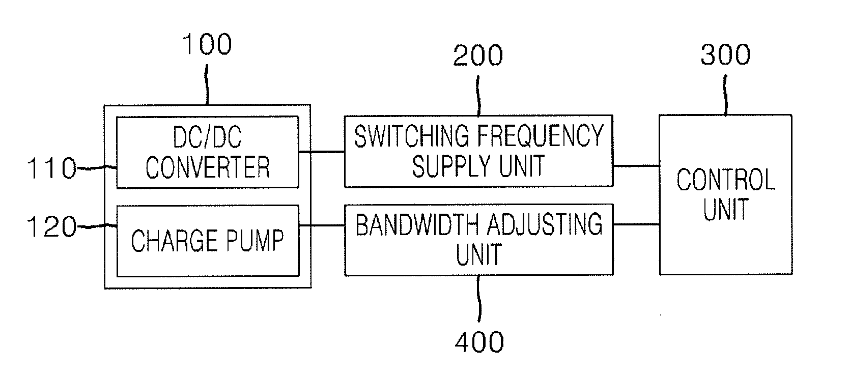
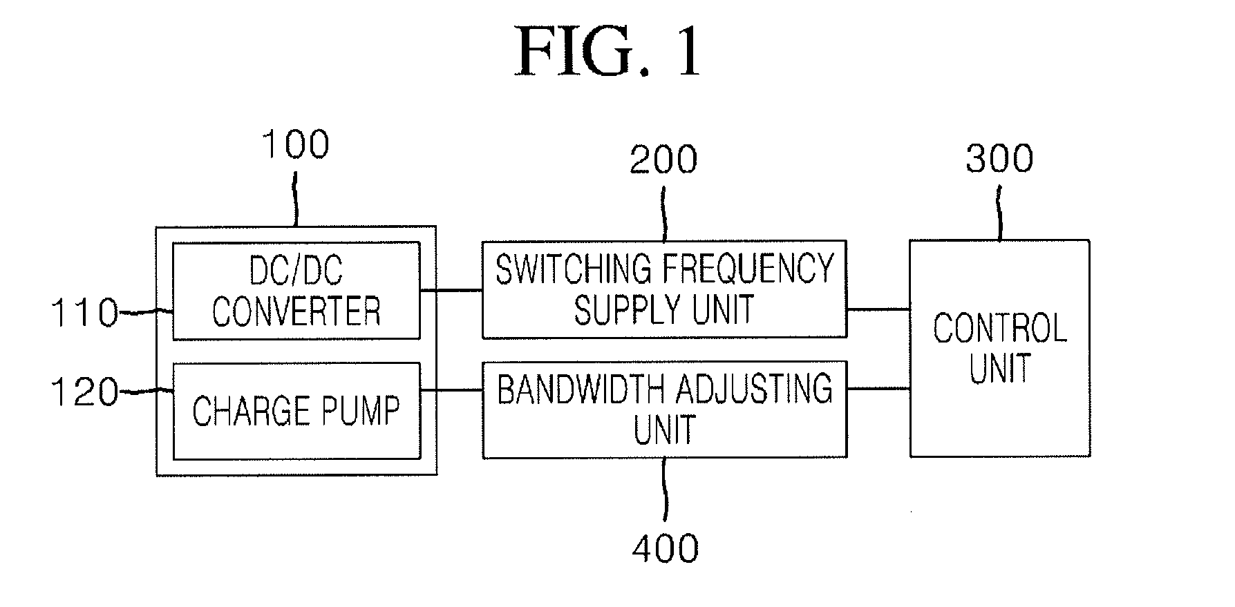
[0025]FIG. 1 is a block diagram of an apparatus for controlling a power source semiconductor in accordance with an embodiment of the present invention.

[0026]Referring to FIG. 1, the apparatus for controlling a power source semiconductor may include a switching frequency supply unit 200, a control unit 300, and a bandwidth adjusting unit 400.

[0027]The switching frequency supply unit 200 may supply reference switchin...


PUM


Abstract

A method for controlling a power source semiconductor may include: supplying, by a switching frequency supply unit, preset respective reference switching frequencies to a plurality of elements which are operated according to a respective switching frequency; sensing, by a control unit, sensing interference in the plurality of elements, based on operations of the elements according to the respective reference switching frequencies; setting, by the control unit, bandwidths for the respective reference switching frequencies when the interference in the plurality of elements is sensed; and increasing, by a bandwidth adjusting unit, bandwidth of the respective reference switching frequencies supplied through the switching frequency supply unit, based on the bandwidths for the respective reference switching frequencies.

Description

CROSS-REFERENCES TO RELATED APPLICATIONS[0001]The present application claims priority to Korean application number 10-2014-0156974, filed on Nov. 12, 2014, which is incorporated by reference in its entirety.BACKGROUND OF THE INVENTION[0002]The present invention relates to a method and apparatus for controlling a power source semiconductor, and more particularly, to a method and apparatus for controlling a power source semiconductor, which is capable of reducing the influence of interference caused by electromagnetic wave noise between elements operating at a fixed switching frequency, thereby preventing malfunctions of the respective elements.[0003]These days, with the development of electronic devices, a large number of parts included in a vehicle rely on the control of the electronic devices, in order to improve the performance of the vehicle. For example, in order to improve the performance of an engine, various sensors are used to achieve the optimal engine efficiency. Therefore...

Claims


Application Information

Patent Timeline
IPC IPC(8): H04B1/69
CPCH04B1/69H02M1/143H02M1/44H02H7/1213H02M1/425H02M3/3376H03K17/785H01L23/24
Inventor LEE, SOON SEOBHA, TAE OKSHIN, JONG HA
Owner HYUNDAI MOBIS CO LTD
Features
  • Generate Ideas
  • Intellectual Property
  • Life Sciences
  • Materials
  • Tech Scout
  • Unparalleled Data Quality
  • Higher Quality Content
  • 60% Fewer Hallucinations
Learn More