Display panel

a display panel and display panel technology, applied in the field of display panels, can solve the problems of reducing the area of the transparent window, affecting the operation so as to improve the transmittance of the display panel, reduce the electrical resistance difference in the fan-out portion, and improve the effect of the display panel transmittan

Active Publication Date: 2016-05-19
SAMSUNG DISPLAY CO LTD
View PDF4 Cites 35 Cited by
  • Summary
  • Abstract
  • Description
  • Claims
  • Application Information

AI Technical Summary

Benefits of technology

[0029]According to example embodiments, a display panel may have a first region (e.g., a low resolution region), a second region (e.g., a high resolution region) and a plurality of wirings extending from the first region to second region. In this case, a first unit pixel having a first area may be disposed in the first region, and a second unit pixel having a second area which may be smaller than the first area may be disposed in the second region. Therefore, the second region may display a high resolution image, and the first region may improve a transmittance of the display panel. Further, the plurality of wirings may have a fan-out portion, and the fan-out portion may have bilateral symmetry, and may have identical length. Therefore, an electrical resistance difference in the fan-out portion may be reduced or prevented, and the display panel may display a high quality image.
[0030]According to comparative embodiments, if a resolution of a display panel increases and an area of the unit pixel decreases at a predetermined panel size, an area of the transparent window may decrease, and a transmittance of the display panel may also degrade. Further, as the resolution of the display panel increases, the number of wirings may also increase, so that a charging time for each wiring may decrease, and a quality of an image of the display panel may degrade. On the other hand, if an area of the transparent window increases in order to improve the transmittance of the display panel, an area of the unit pixel may also increase, and it is hard to implement a high resolution image. In order to solve the above problems, the display panel 100 according to example embodiments may include the first region (I) (that is, a low resolution region) and the second region (II) (that is, a high resolution region). Therefore, a transmittance of the display panel 100 may be improved due to the first transparent window 124 in the first region (I), and the second region (II) may display the high resolution image. That is, the display panel 100 may have an improved transmittance and may display the high resolution image simultaneously. Further, the display panel 100 may use either the first region (I) or the second region (II) selectively, so that a power consumption of the display panel 100 may decrease.
[0031]Further, the display panel 100 may include the wiring groups 140 which may have the plurality of wirings 140a, 140b, 140c, 140d, 140e and 140f extending from the first region (I) to the second region (II). The plurality of wirings 140a, 140b, 140c, 140d, 140e and 140f may have a fan-out portion at the interface between the first region (I) and the second region (II), and the fan-out portion may have bilateral symmetry and may have identical length. Therefore, an electrical resistance difference between the plurality of wirings may be reduced or prevented, and the display panel may display a high quality image.

Problems solved by technology

Therefore, it is hard to implement a high resolution and a high transmittance simultaneously.
According to comparative embodiments, if a resolution of a display panel increases and an area of the unit pixel decreases at a predetermined panel size, an area of the transparent window may decrease, and a transmittance of the display panel may also degrade.
Further, as the resolution of the display panel increases, the number of wirings may also increase, so that a charging time for each wiring may decrease, and a quality of an image of the display panel may degrade.
On the other hand, if an area of the transparent window increases in order to improve the transmittance of the display panel, an area of the unit pixel may also increase, and it is hard to implement a high resolution image.

Method used


Image

  • Display panel
  • Display panel
  • Display panel

Examples


Embodiment Construction

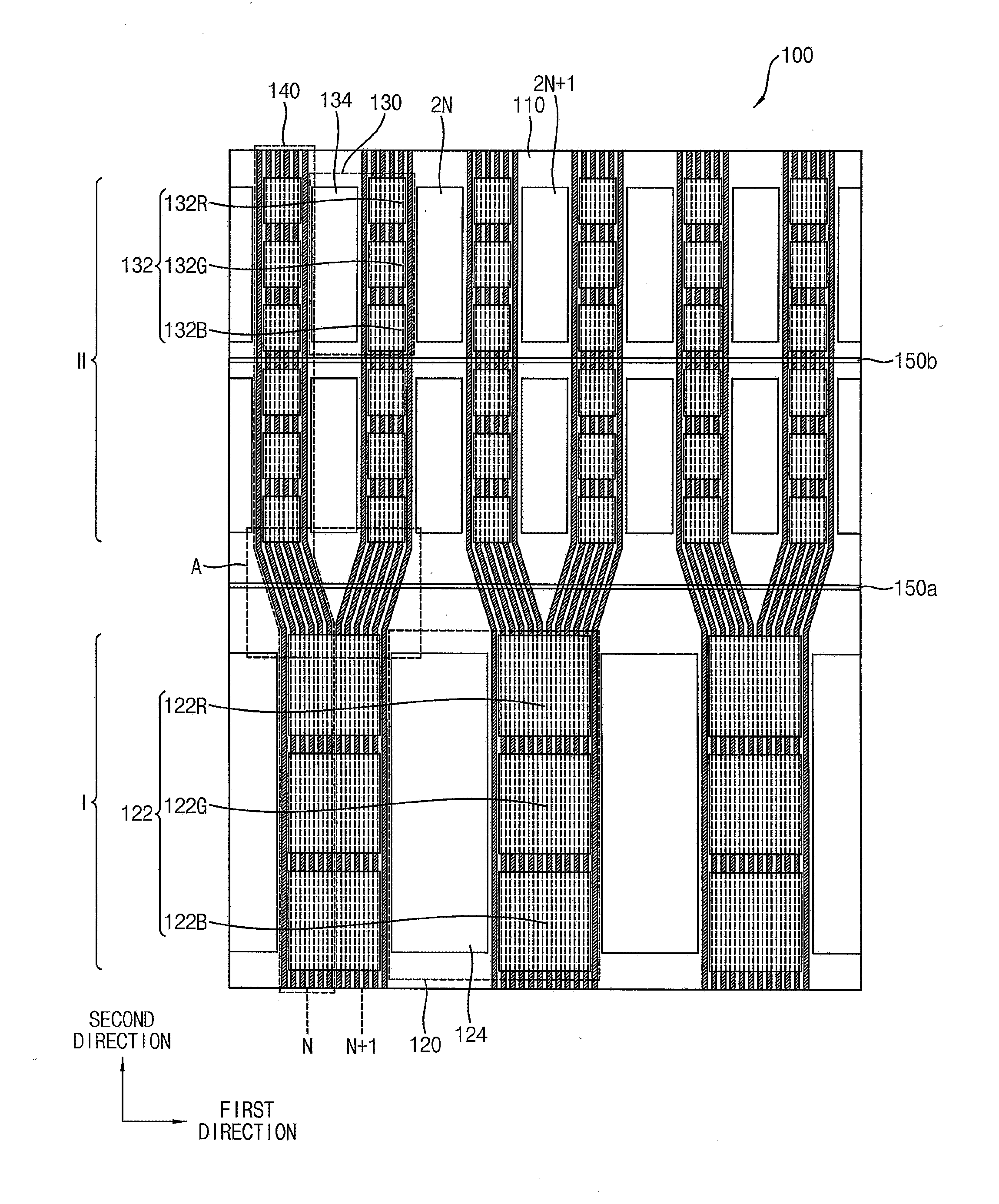
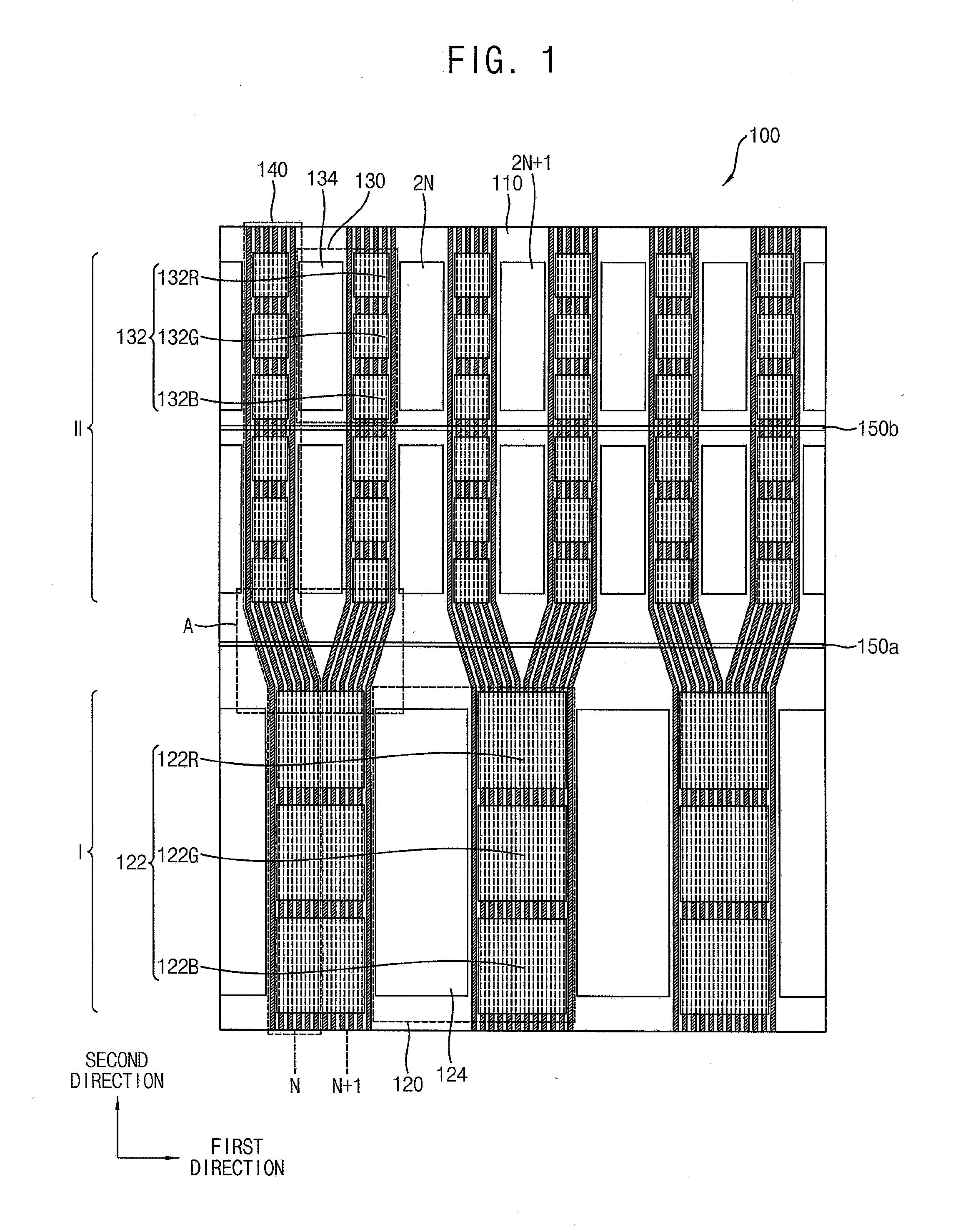
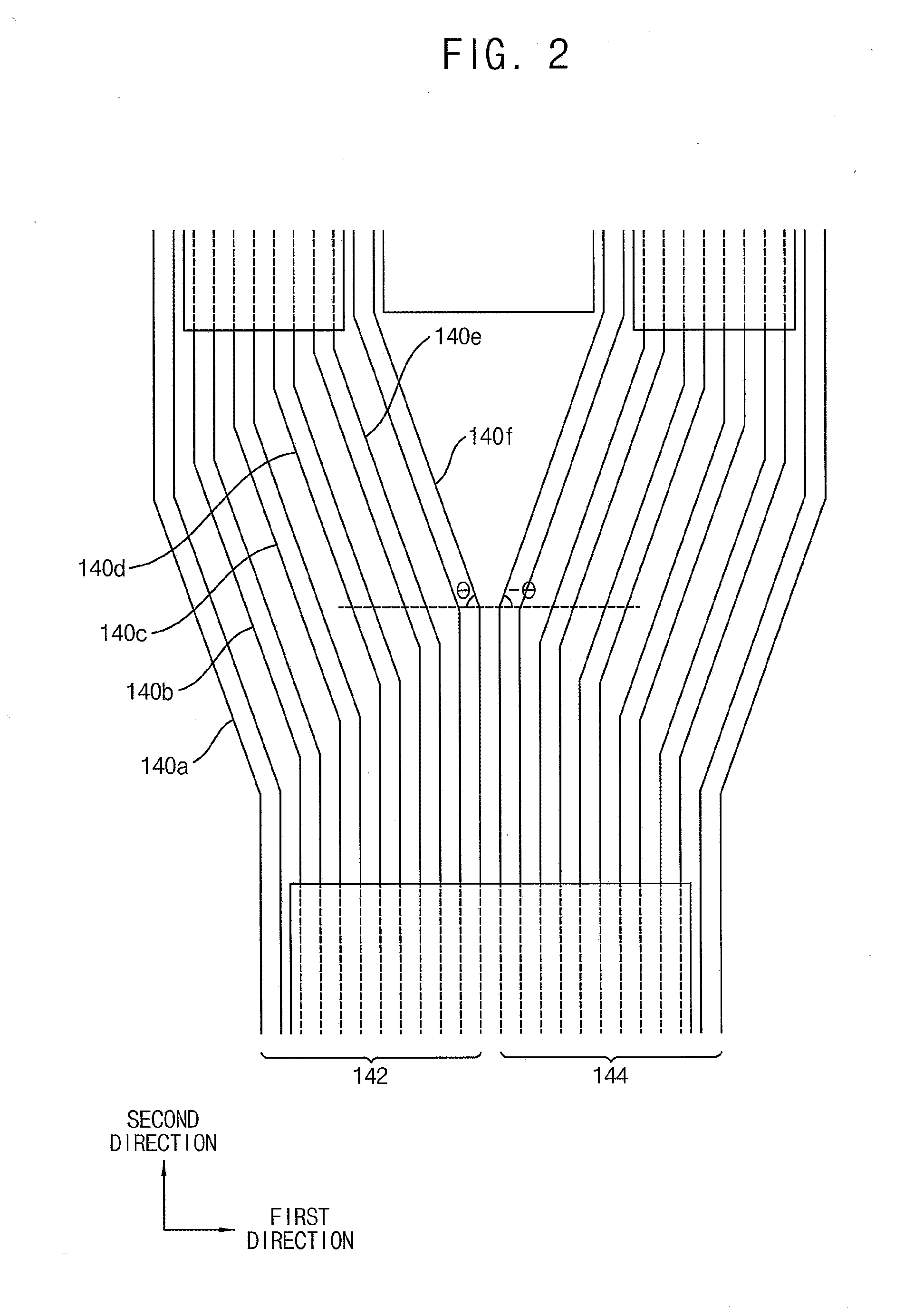
[0042]The example embodiments are described more fully hereinafter with reference to the accompanying drawings. The invention may, however, be embodied in many different forms and should not be construed as limited to the example embodiments set forth herein. In the drawings, the sizes and relative sizes of layers and regions may be exaggerated for clarity.

[0043]It will be understood that when an element or layer is referred to as being “on,”“connected to” or “coupled to” another element or layer, it can be directly on, connected or coupled to the other element or layer or intervening elements or layers may be present between the element or layer and the another element or layer. In contrast, when an element is referred to as being “directly on,”“directly connected to” or “directly coupled to” another element or layer, there are no intervening elements or layers present between the element or layer and the another element or layer. Like or similar reference numerals refer to like or...


PUM


Abstract

A display panel is disclosed. The display panel includes a substrate, a plurality of first unit pixel and a plurality of second unit pixel. The substrate includes a first region and a second region extending in a first direction. The plurality of first unit pixels is disposed in the first region of the substrate. The first unit pixel has a first area. The plurality of second unit pixel is disposed in the second region of the substrate. The second unit pixel has a second area which is smaller than the first area.

Description

CROSS REFERENCE TO RELATED APPLICATION[0001]This application claims priority under 35 USC §119 to Korean Patent Application No. 2014-0160457 filed on Nov. 18, 2014 in the Korean Intellectual Property Office (KIPO), the disclosures of which are herein incorporated by reference in their entireties.BACKGROUND[0002]1. Technical Field[0003]Example embodiments relate to a display panel. More particularly, example embodiments relate to a transparent display panel including a plurality of pixels and a plurality of transparent windows.[0004]2. Description of the Related Art[0005]Recently, a transparent organic light emitting display device has been studied. The transparent organic light emitting display device can transmit an image of an object behind the organic light emitting display device when the organic light emitting display device operates in an “OFF” state. In an “ON” state of the organic light emitting display device, the organic light emitting display device may display an image i...

Claims


Application Information

Patent Timeline
Patent Type & Authority Applications(United States)
IPC IPC(8): H01L27/32
CPCH01L27/3288H01L27/3267H01L27/3276H01L27/326H01L27/3286H01L27/3279H10K59/352H10K59/353H10K59/121H10K59/131H10K59/1315H10K59/128H10K59/176H10K59/179
Inventor KIM, DONG-GYUCHOI, JOON-HOOMOON, SUNG-JAE
Owner SAMSUNG DISPLAY CO LTD
Why Eureka
Try Eureka