

Semiconductor device
a technology of semiconductor devices and semiconductors, applied in semiconductor devices, semiconductor/solid-state device details, electrical apparatus, etc., can solve problems such as increased thermal resistance, insufficient pressure on insulating substrates, and inability to solve problems
- Summary
- Abstract
- Description
- Claims
- Application Information
AI Technical Summary
Benefits of technology
Problems solved by technology
Method used
Image

Examples
first preferred embodiment
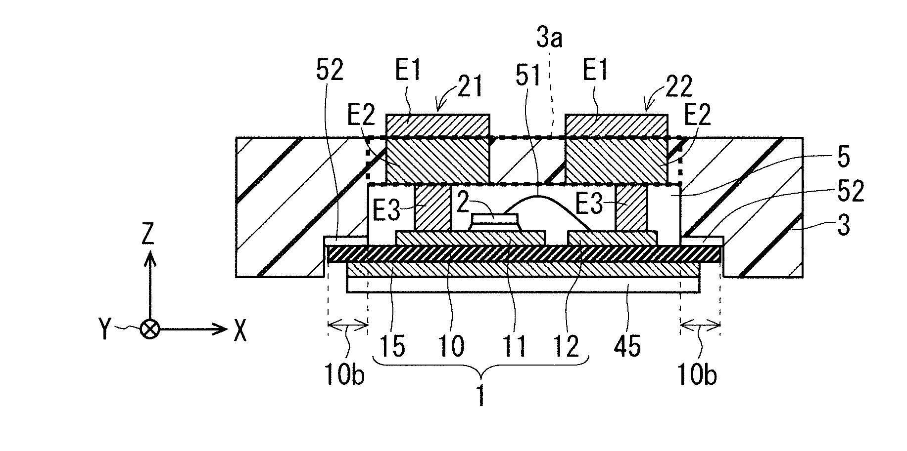
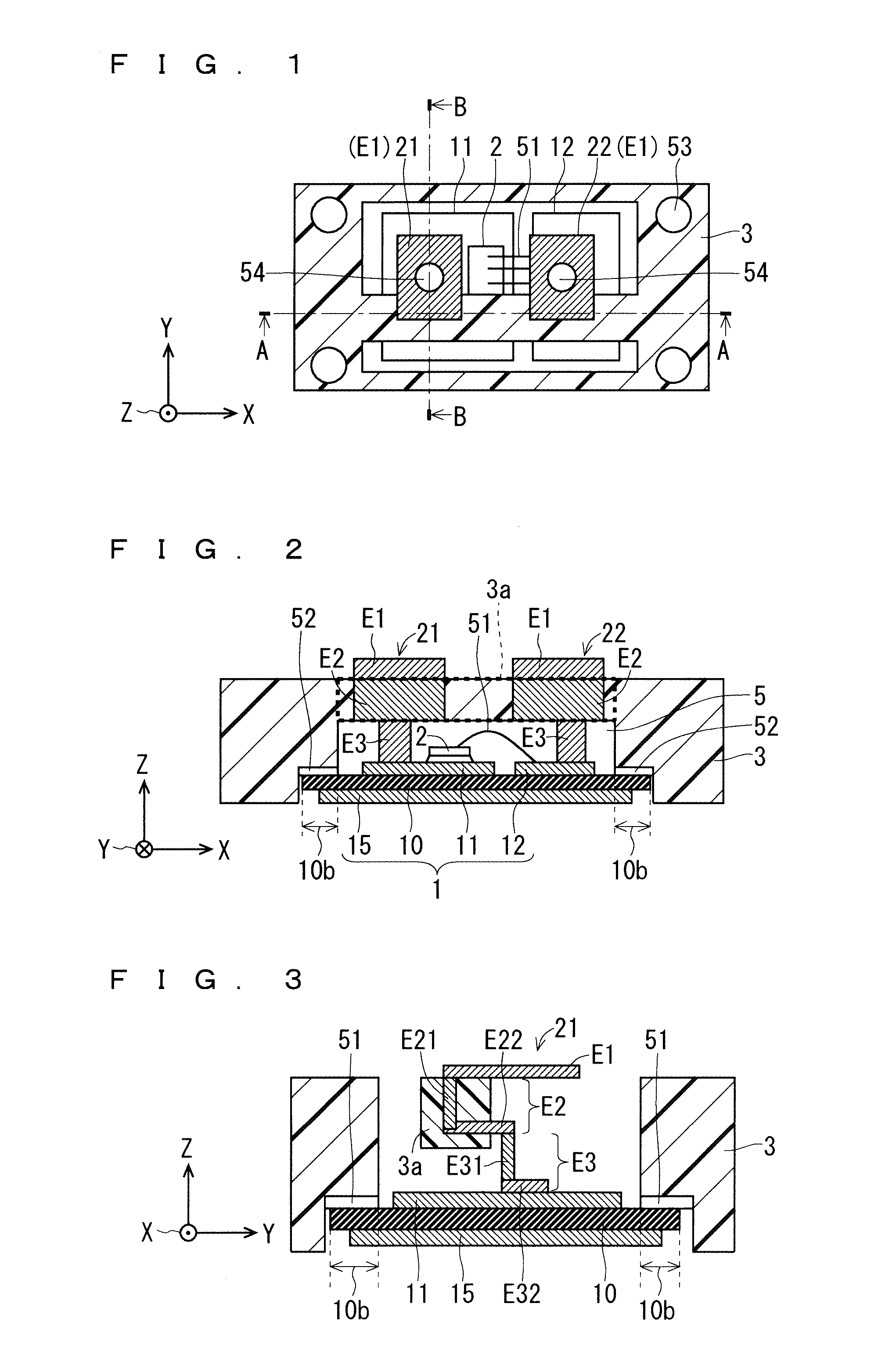
[0034]FIG. 1 is a plan view of an upper surface structure of a power module (semiconductor device) according to a first preferred embodiment of the present invention. FIG. 2 is a cross-sectional view of a cross-sectional structure taken along a cross section A-A in FIG. 1. FIG. 3 is a cross-sectional view of a cross-sectional structure taken along a cross section B-B in FIG. 1. An XYZ orthogonal coordinate system is illustrated in each of FIGS. 1 to 3. Hereinafter, the power module of the first preferred embodiment will be described with reference to FIGS. 1 to 3.
[0035]An insulating substrate 1 is constituted by an insulating plate 10, wiring patterns 11 and 12, and a backside electrode 15 (internal electrode). The wiring patterns 11 and 12 are formed on the front surface of the insulating plate 10, and the backside electrode 15 is formed on the back surface of the insulating plate 10.
[0036]On the wiring pattern 11 of the insulating substrate 1, a semiconductor element 2 made of sil...
second preferred embodiment
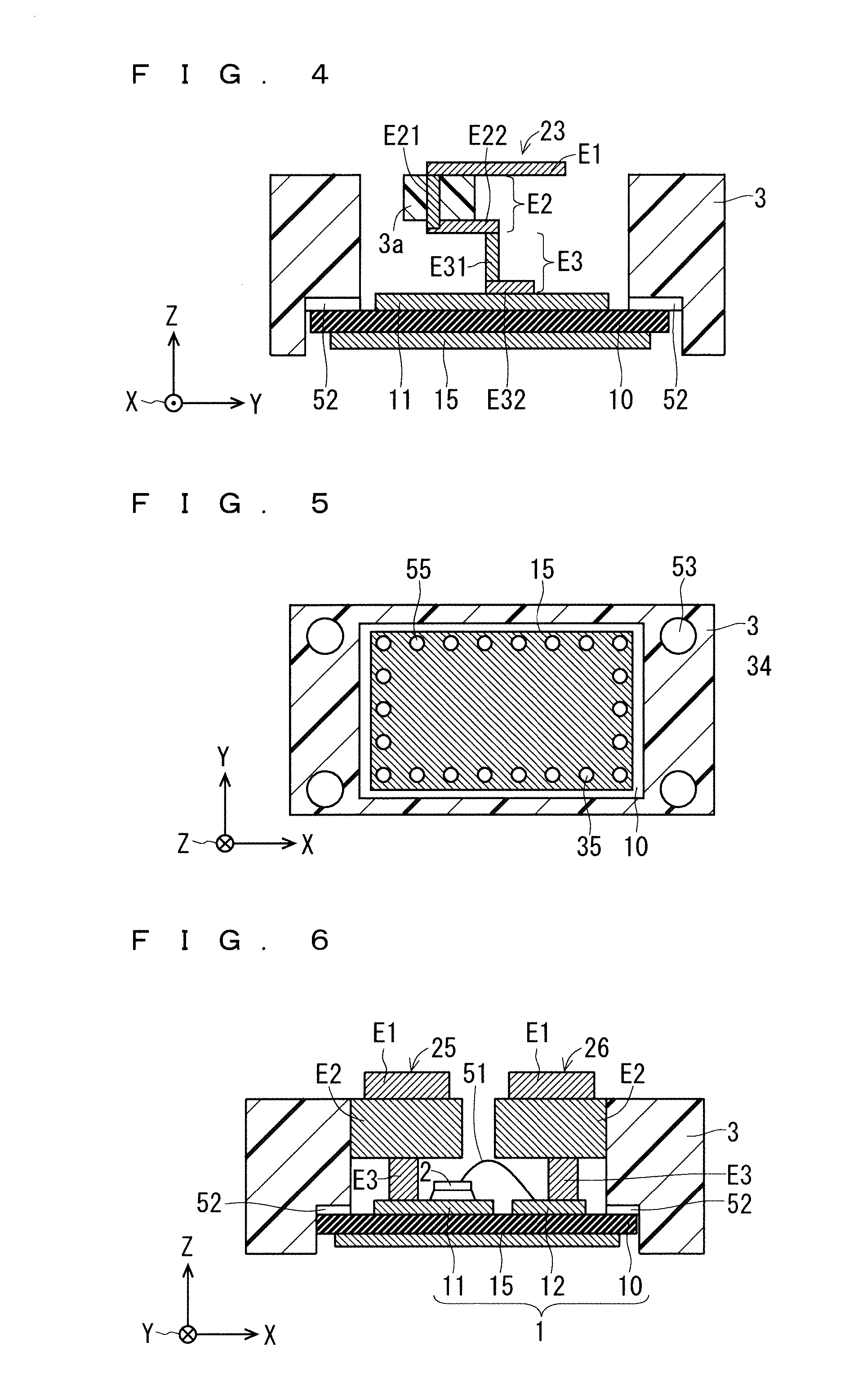
[0056]FIG. 4 is a cross-sectional view of a cross-sectional structure of a power module according to a second preferred embodiment of the present invention. An XYZ orthogonal coordinate system is illustrated in FIG. 4. Note that FIG. 4 corresponds to the cross section B-B in FIG. 1 of the first preferred embodiment, the same reference numerals have been given to constituent elements that are similar to those of the first preferred embodiment, and descriptions thereof have been appropriately omitted.
[0057]As illustrated in FIG. 4, a feature of the power module of the second preferred embodiment is that at least one of the external electrodes 21 and 22 of the first preferred embodiment is replaced by an external electrode 23. Similarly to the external electrodes 21 and 22 of the first preferred embodiment, the external electrode 23 in the power module of the second preferred embodiment is constituted by an external connection part E1, an electrode insertion part E2, and a substrate co...
third preferred embodiment
[0060]FIG. 5 is a plan view of the underside structure of a power module according to a third preferred embodiment of the present invention. An XYZ orthogonal coordinate system is illustrated in FIG. 5. Note that the same reference numerals have been given to constituent elements that are similar to those of the first preferred embodiment, and descriptions thereof have been appropriately omitted.
[0061]As illustrated in FIG. 5, a feature of the power module of the third preferred embodiment is that a plurality of dimples (recessed parts) 55, each being recessed from the other region toward the front surface side (one main surface side) of the insulating substrate 1, are provided in the outer peripheral portion of the underside (surface on the other main surface side) of the backside electrode 15. These dimples 55 alleviate the stress placed on the boundary of the backside electrode 15 and thereby reduce the occurrence of a phenomenon in which cracks occurs in the insulating plate 10 ...
PUM
 Abstract
Description
Claims
Application Information