
Liquid crystal panel and manufacture method thereof

a technology of liquid crystal panels and manufacturing methods, applied in the field of display technology, can solve the problems of reducing production efficiency and prolonging the array process time, and achieve the effect of reducing the probability of mm mura occurrence and lowering alignment demands

Active Publication Date: 2016-06-16
SHENZHEN CHINA STAR OPTOELECTRONICS TECH CO LTD
View PDF5 Cites 5 Cited by
  • Summary
  • Abstract
  • Description
  • Claims
  • Application Information

AI Technical Summary

Benefits of technology

The present invention provides a liquid crystal panel and a manufacture method that can reduce the occurrence of a visual artifact called "MM mura" and lower the alignment demands for the upper and lower substrates during the lamination process. This results in a simplified process, savings in masks, and increased production efficiency. Additionally, the invention utilizes color resist material to form a photospacer layer at the side of the array substrate, which further reduces the patent text's technical effects.

Problems solved by technology

However, the photospacer is formed at the one side of the TFT array substrate, one photo process is added at the one side of the TFT array substrate, which can extend the Array process time and diminish the production efficiency.

Method used


Image

  • Liquid crystal panel and manufacture method thereof
  • Liquid crystal panel and manufacture method thereof
  • Liquid crystal panel and manufacture method thereof

Examples


first embodiment

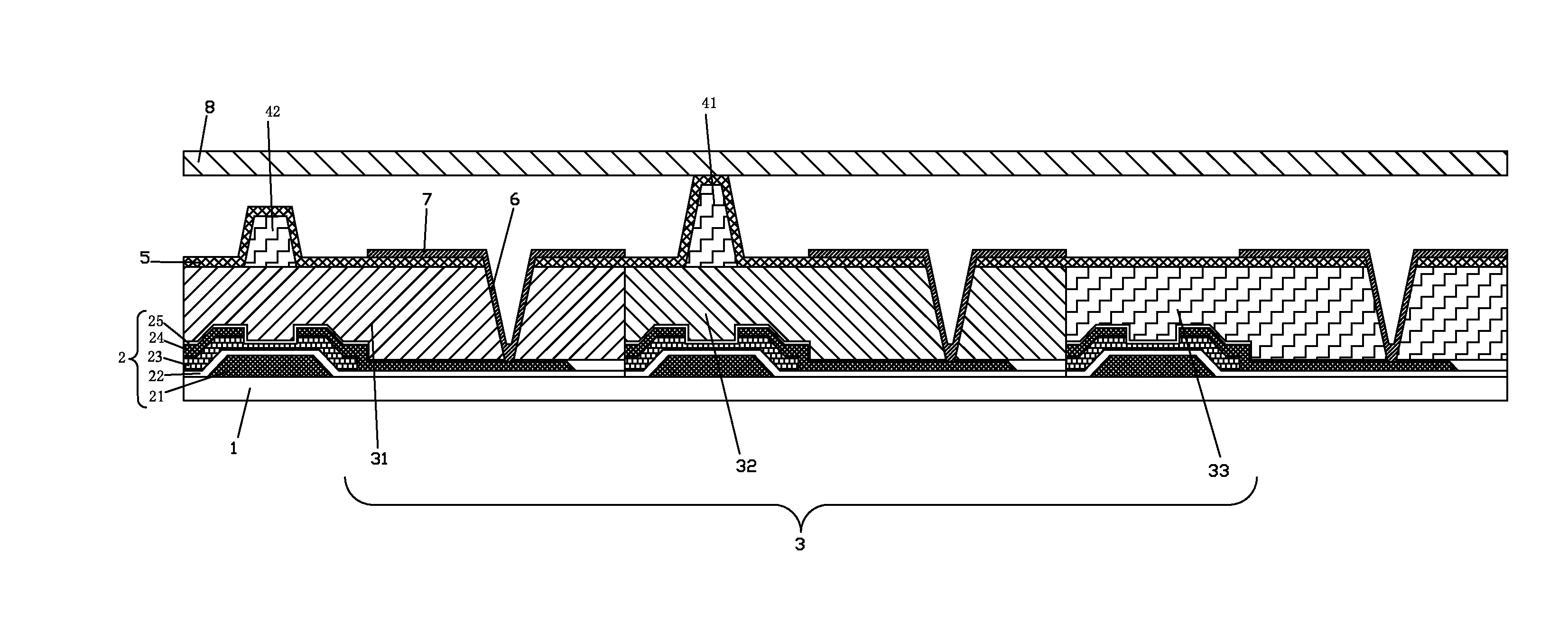
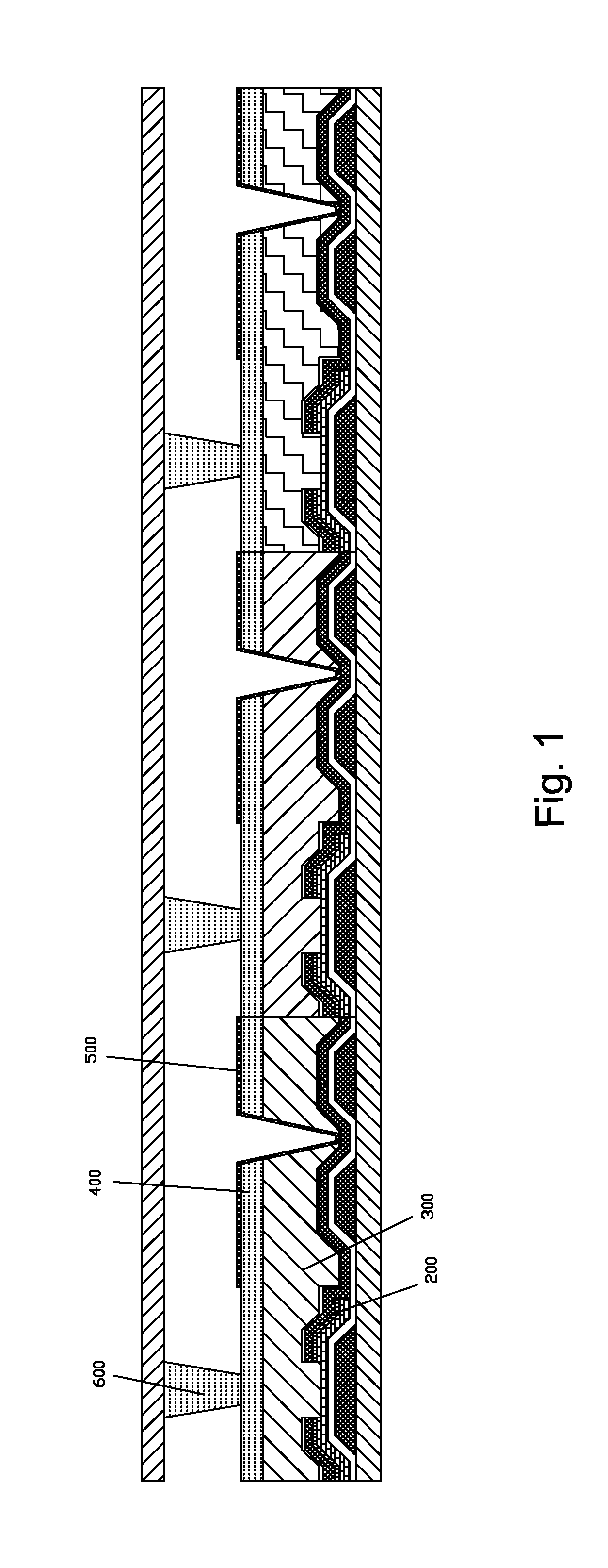
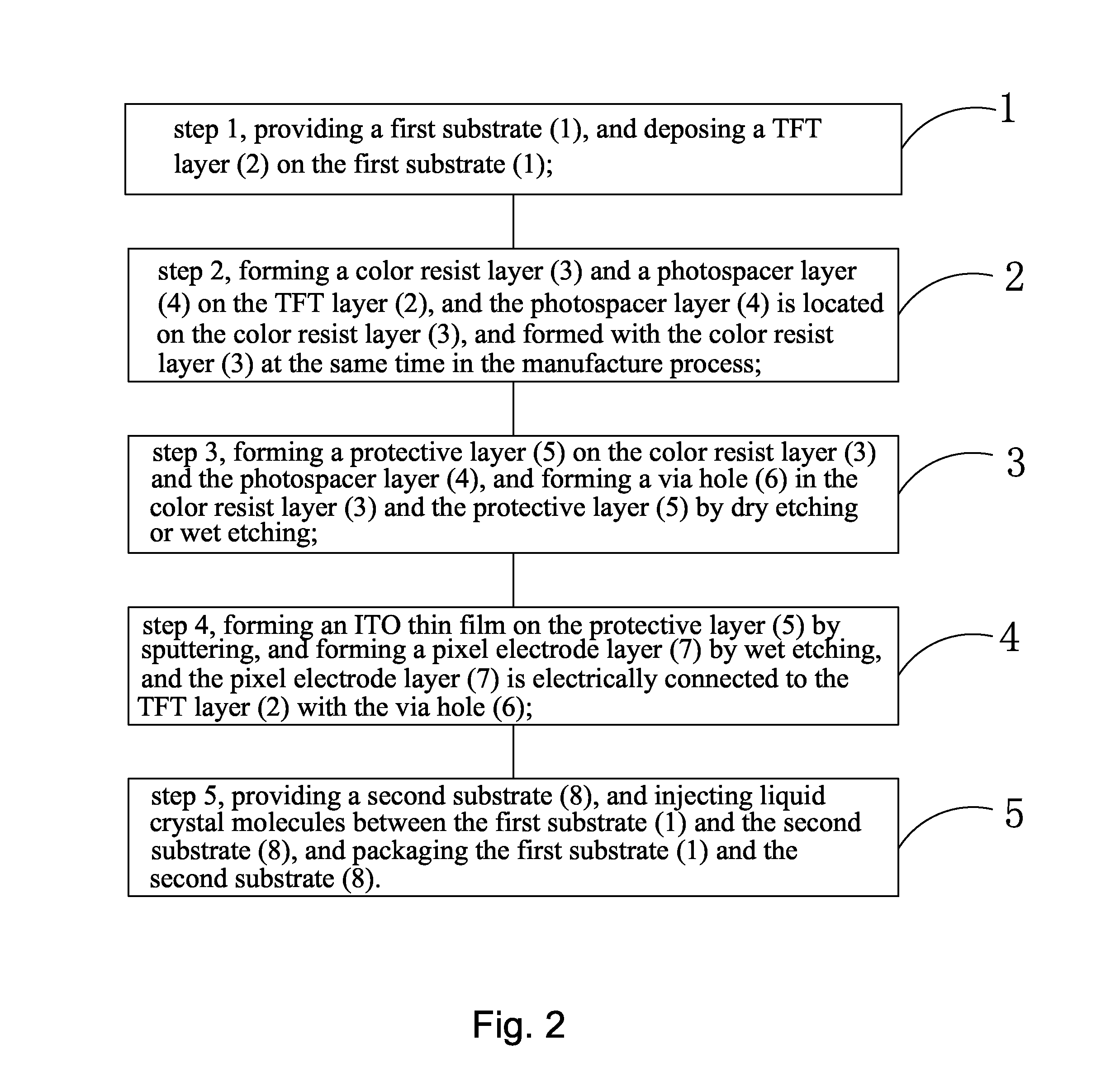
[0051]Please refer to FIG. 3, which is a structural diagram of a liquid crystal panel according to the present invention. As shown in FIG. 3, the present invention provides a liquid crystal panel, comprising a first substrate 1, a TFT layer 2 located on the first substrate 1, a color resist layer 3 located on the TFT layer 2, a photospacer layer 4 located on the color resist layer 3, a protective layer 5 located on the color resist layer 3 and the photospacer layer 4, a via hole 6 penetrating the color resist layer 3 and the protective layer 5, a pixel electrode layer 7 formed on the protective layer 5 and electrically connected to the TFT layer 2 with the via hole 6 and a second substrate 8 oppositely located to the first substrate 1. One or more color resist material in the photospacer layer 4 and the color resist layer 3 are the same, and the photospacer layer 4 and the color resist layer 3 are formed at the same time during a manufacture process.

[0052]The color resist layer 3 co...

second embodiment

[0071]In the liquid crystal panel according to the present invention, the color resist layer 3 comprises a first color resist 31, a second color resist 32 and a third color resist 33 which are sequentially arranged, and the photospacer layer 4 comprises a main photospacer 41 and a sub photospacer 42, and a height of the main photospacer 41 is larger than a height of the sub photospacer 42.

[0072]Both the main photospacer 41 and the sub photospacer 42 of the photospacer layer 4 are located on the first color resist 31. Material of the main photospacer 41, material of the sub photospacer 42 and material of the second color resist 32 in the color resist layer 3 are the same, and the three are formed in the same photo process.

[0073]The manufacture method of the liquid crystal panel according to the second embodiment of the present invention is similar with the manufacture method of the liquid crystal panel according to the first embodiment of the present invention. The difference is that...

third embodiment

[0079]In the liquid crystal panel according to the present invention, the color resist layer 3 comprises a first color resist 31, a second color resist 32 and a third color resist 33 which are sequentially arranged, and the photospacer layer 4 comprises a main photospacer 41 and a sub photospacer 42, and a height of the main photospacer 41 is larger than a height of the sub photospacer 42.

[0080]The sub photospacer 42 is located on the first color resist 31, and the main photospacer 41 is located on the second color resist 32, and material of the main photospacer 41, material of the sub photospacer 42 and material of the third color resist 33 are the same, and the three are formed in the same photo process.

[0081]The manufacture method of the liquid crystal panel according to the third embodiment of the present invention is similar with the manufacture method of the liquid crystal panel according to the first embodiment of the present invention. The difference is that the specific ste...


PUM


Abstract

The present invention provides a liquid crystal panel and a manufacture method thereof. The liquid crystal panel comprises: a first substrate (1), a TFT layer (2) located on the first substrate (1), a color resist layer (3) located on the TFT layer (2), a photospacer layer (4) located on the color resist layer (3), a protective layer (5) located on the color resist layer (3) and the photospacer layer (4), a via hole (6) penetrating the color resist layer (3) and the protective layer (5), a pixel electrode layer (7) formed on the protective layer (5) and electrically connected to the TFT layer (2) with the via hole (6) and a second substrate (8) oppositely located to the first substrate (1), and one or more color resist material in the photospacer layer (4) and the color resist layer (3) are the same, and the photospacer layer (4) and the color resist layer (3) are formed at the same time during a manufacture process.

Description

FIELD OF THE INVENTION[0001]The present invention relates to a display technology field, and more particularly to a liquid crystal panel and a manufacture method thereof.BACKGROUND OF THE INVENTION[0002]With the development of display technology, the flat panel device, such as Liquid Crystal Display (LCD) possesses advantages of high image quality, power saving, thin body and wide application scope. Thus, it has been widely applied in various consumer electrical products, such as mobile phone, television, personal digital assistant, digital camera, notebook, laptop, and becomes the major display device.[0003]Most of the liquid crystal displays on the present market are back light type liquid crystal displays, which comprise a liquid crystal display panel and a back light module. The working principle of the liquid crystal display panel is to locate liquid crystal molecules between two parallel glass substrates, and a plurality of vertical and horizontal tiny electrical wires are bet...

Claims


Application Information

Patent Timeline
IPC IPC(8): G02F1/1339G02F1/1341G02F1/1362H01L27/12G02F1/1368
CPCG02F1/13394H01L27/124H01L27/1292G02F2001/136222G02F1/136227G02F1/1341G02F2001/13396G02F1/1368G02F1/133351G02F1/1339G02F1/13398H01L27/1248G02F1/13396G02F1/136222G02F2201/123H01L27/1259
Inventor SONG, LIWANGXU, YONG
Owner SHENZHEN CHINA STAR OPTOELECTRONICS TECH CO LTD
Learn More