Integrated device package comprising photo sensitive fill between a substrate and a die

Inactive Publication Date: 2016-06-16
QUALCOMM INC
View PDF7 Cites 7 Cited by
  • Summary
  • Abstract
  • Description
  • Claims
  • Application Information

AI Technical Summary

Benefits of technology

This patent describes an integrated device package that includes a photo sensitive fill between a substrate and a die. The package includes a die with a die interconnect, a substrate with a dielectric layer and a substrate interconnect, and a conductive interconnect within the fill. The conductive interconnect is coupled to the die interconnect and the substrate interconnect. The technical effect of this patent is to provide a more efficient and reliable method for coupling a die to a substrate, which can improve the performance and reliability of the integrated device package.

Problems solved by technology

An elongated solder 123 is problematic in a package that includes high density, low pitch and / or low spacing interconnects because the elongated solder 123 may make physical contact with a nearby solder, pillar and / or interconnect causing a short in the package.
An elongated solder 200 is problematic in a package that includes high density, low pitch and / or low spacing interconnects because the elongated solder 200 may make physical contact with a nearby solder, pillar and / or interconnect causing a short in the package.
This results in unnecessary material (e.g., too much solder 323), resulting in higher cost of the integrated package.

Method used


Image

  • Integrated device package comprising photo sensitive fill between a substrate and a die
  • Integrated device package comprising photo sensitive fill between a substrate and a die
  • Integrated device package comprising photo sensitive fill between a substrate and a die

Examples


Embodiment Construction

[0038]In the following description, specific details are given to provide a thorough understanding of the various aspects of the disclosure. However, it will be understood by one of ordinary skill in the art that the aspects may be practiced without these specific details. For example, circuits may be shown in block diagrams in order to avoid obscuring the aspects in unnecessary detail. In other instances, well-known circuits, structures and techniques may not be shown in detail in order not to obscure the aspects of the disclosure.

OVERVIEW

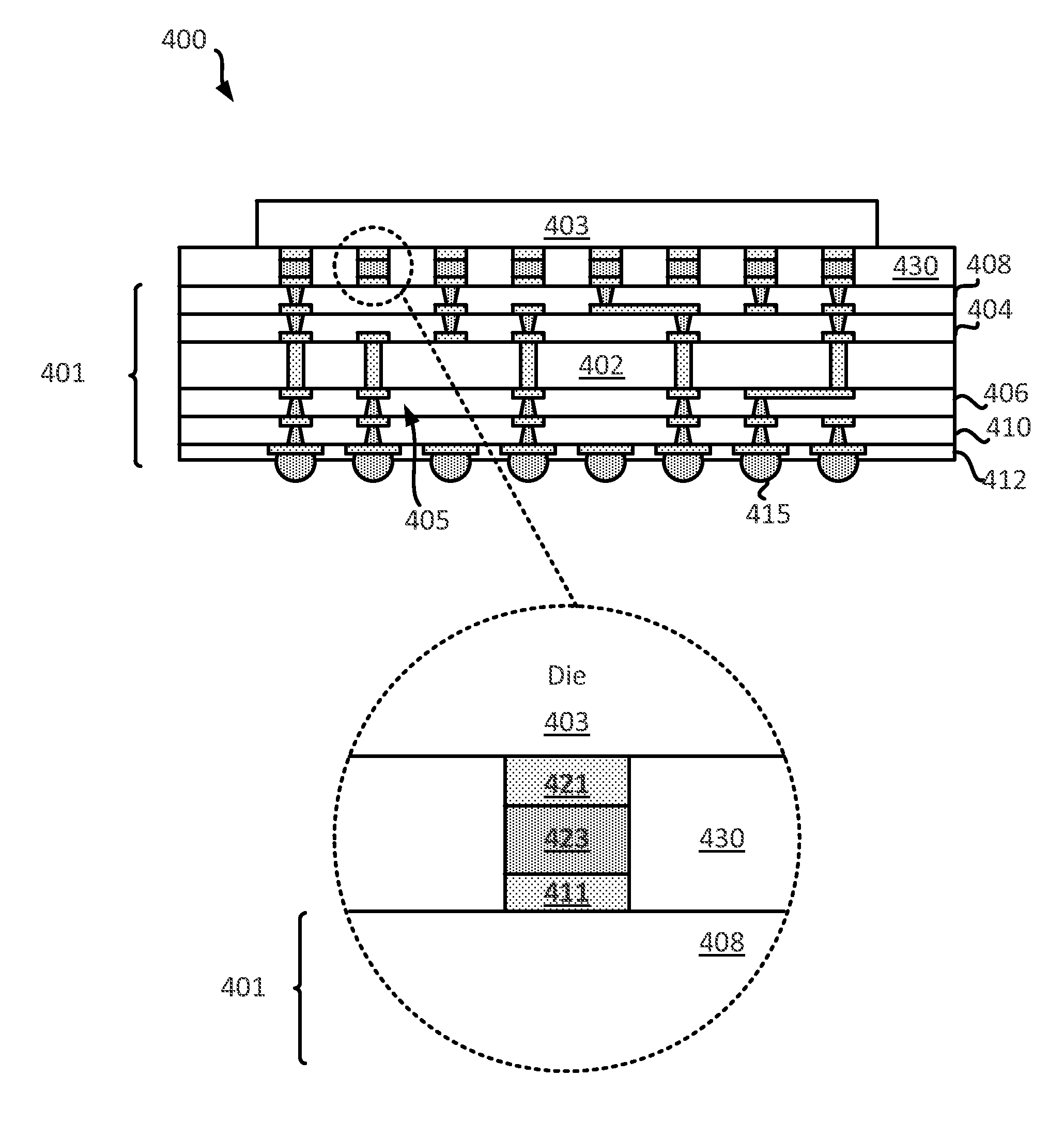
[0039]Some features pertain to an integrated device package that includes a die, a substrate, a fill and a conductive interconnect. The die includes a pillar (e.g., die interconnect), where the pillar has a first pillar width. The substrate (e.g., package substrate, interposer) includes a dielectric layer and a substrate interconnect (e.g., surface interconnect, embedded interconnect). The fill is located between the die and the substrate. The con...


PUM


Abstract

An integrated device package that includes a die, a substrate, a fill and a conductive interconnect. The die includes a pillar, where the pillar has a first pillar width. The substrate (e.g., package substrate, interposer) includes a dielectric layer and a substrate interconnect (e.g., surface interconnect, embedded interconnect). The fill is located between the die and the substrate. The conductive interconnect is located within the fill. The conductive interconnect includes a first interconnect width that is about the same or less than the first pillar width. The conductive interconnect is coupled to the pillar and the substrate interconnect. The fill is a non-conductive photosensitive material. The fill is a photosensitive film. The substrate interconnect includes a second interconnect width that is equal or greater than the first pillar width. The conductive interconnect includes one of at least a paste, a solder and / or an enhanced solder comprising a polymeric material.

Description

CLAIM OF PRIORITY / CLAIM OF BENEFIT[0001]The present application claims priority to U.S. Provisional Application No. 62 / 091,400 titled “Integrated Device Package Comprising Photo Sensitive Fill Between a Substrate and a Die”, filed Dec. 12, 2014, which is hereby expressly incorporated by reference herein.BACKGROUND[0002]1. Field[0003]Various features relate to an integrated device package that includes a photo sensitive fill between a substrate and a die.[0004]2. Background[0005]FIG. 1 illustrates a conventional configuration of an integrated package that includes a die. Specifically, FIG. 1 illustrates an integrated device package 100 that includes a package substrate 101, a die 103, and a fill 130. The package substrate 101 includes several dielectric layers (e.g., dielectric layer 102), several interconnects (e.g., traces, vias, pads) 105, and a set of solder balls 115. The package substrate 101 may include an interconnect 111. The interconnect 111 may be a surface interconnect lo...

Claims


Application Information

Patent Timeline
IPC IPC(8): H01L23/528H01L23/31H01L23/00H01L23/522H01L23/498
CPCH01L23/5283H01L23/5226H01L23/49827H01L23/49838H01L24/81H01L24/17H01L23/3157H01L2224/16227H01L2224/81801H01L2924/2064H01L24/11H01L24/13H01L24/16H01L24/27H01L24/29H01L24/73H01L24/92H01L2224/0347H01L2224/0346H01L2224/0345H01L2224/03452H01L2224/0348H01L2224/1111H01L24/03H01L24/83H01L2224/03602H01L2224/05546H01L2224/05571H01L2224/05647H01L2224/11334H01L2224/13007H01L2224/131H01L2224/13147H01L2224/16014H01L2224/16237H01L2224/16238H01L2224/29006H01L2224/73104H01L2224/73204H01L2224/81101H01L2224/81191H01L2224/81192H01L2224/83191H01L2224/83192H01L2224/05568H01L2224/03914H01L2224/27438H01L2224/11438H01L2224/2711H01L2224/16111H01L2224/16013H01L2924/014H01L2924/00014H01L2924/00012
Inventor NOVESKI, VLADIMIRSHAH, MILIND PRAVINKUMAR, RAJNEESH
Owner QUALCOMM INC
Why Eureka
Try Eureka