
Method and Circuit Arrangement for Protecting Against Scanning of an Address Space

a technology of address space and circuit arrangement, applied in the field of integrated electronic circuits, can solve problems such as false information, inability or no longer possible to ascertain

Active Publication Date: 2016-07-14
SIEMENS AG OESTERR
View PDF28 Cites 5 Cited by
  • Summary
  • Abstract
  • Description
  • Claims
  • Application Information

AI Technical Summary

Benefits of technology

The patent aims to provide a method and circuit arrangement that can prevent unauthorized access to an integrated electronic circuit by blocking the scanning of its address space. This approach ensures that the structure and functions of the circuit cannot be derived from the results of the address-space scan.

Problems solved by technology

The address-space scan provides no information or no analyzable information or falsified information from which it is not possible or no longer possible to ascertain the circuit functions.

Method used


Image

  • Method and Circuit Arrangement for Protecting Against Scanning of an Address Space
  • Method and Circuit Arrangement for Protecting Against Scanning of an Address Space
  • Method and Circuit Arrangement for Protecting Against Scanning of an Address Space

Examples


Embodiment Construction

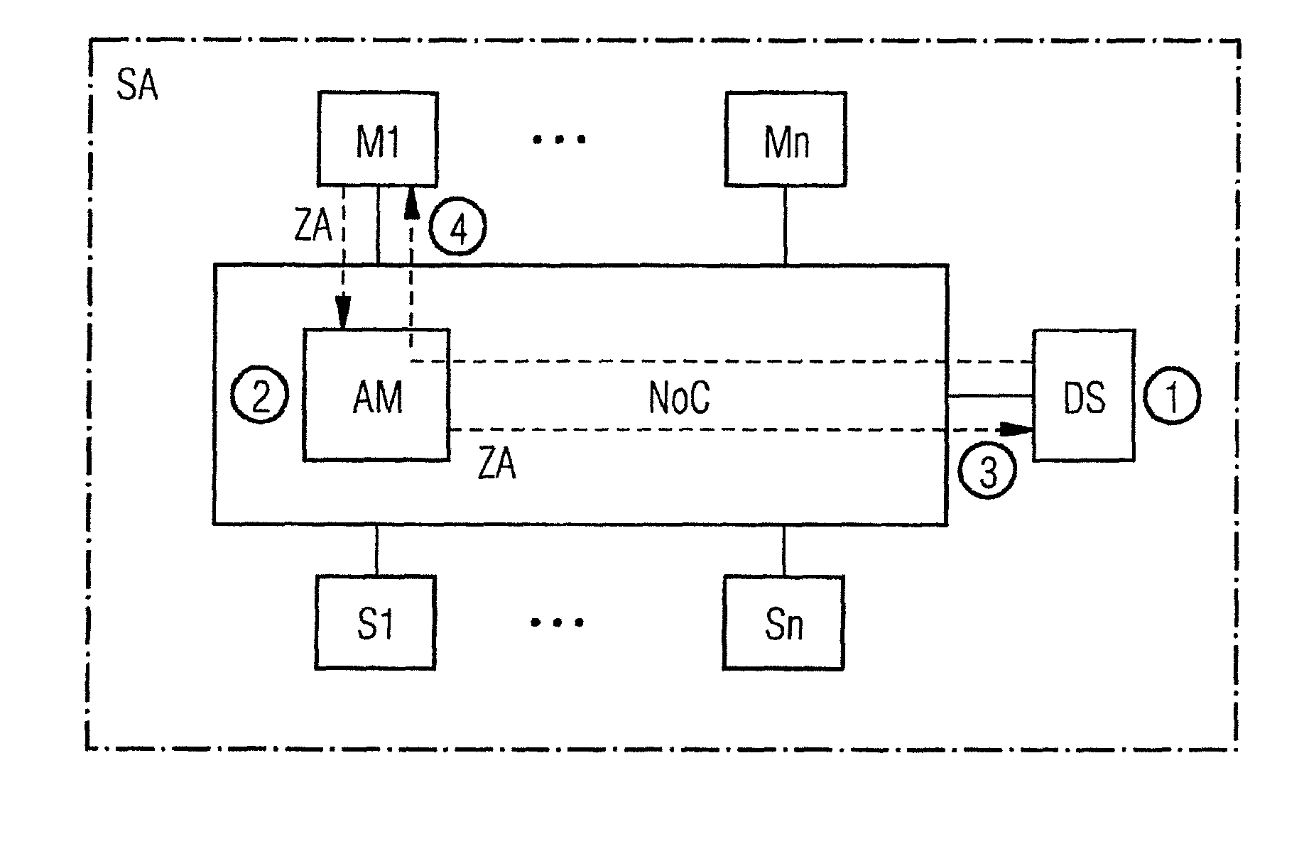
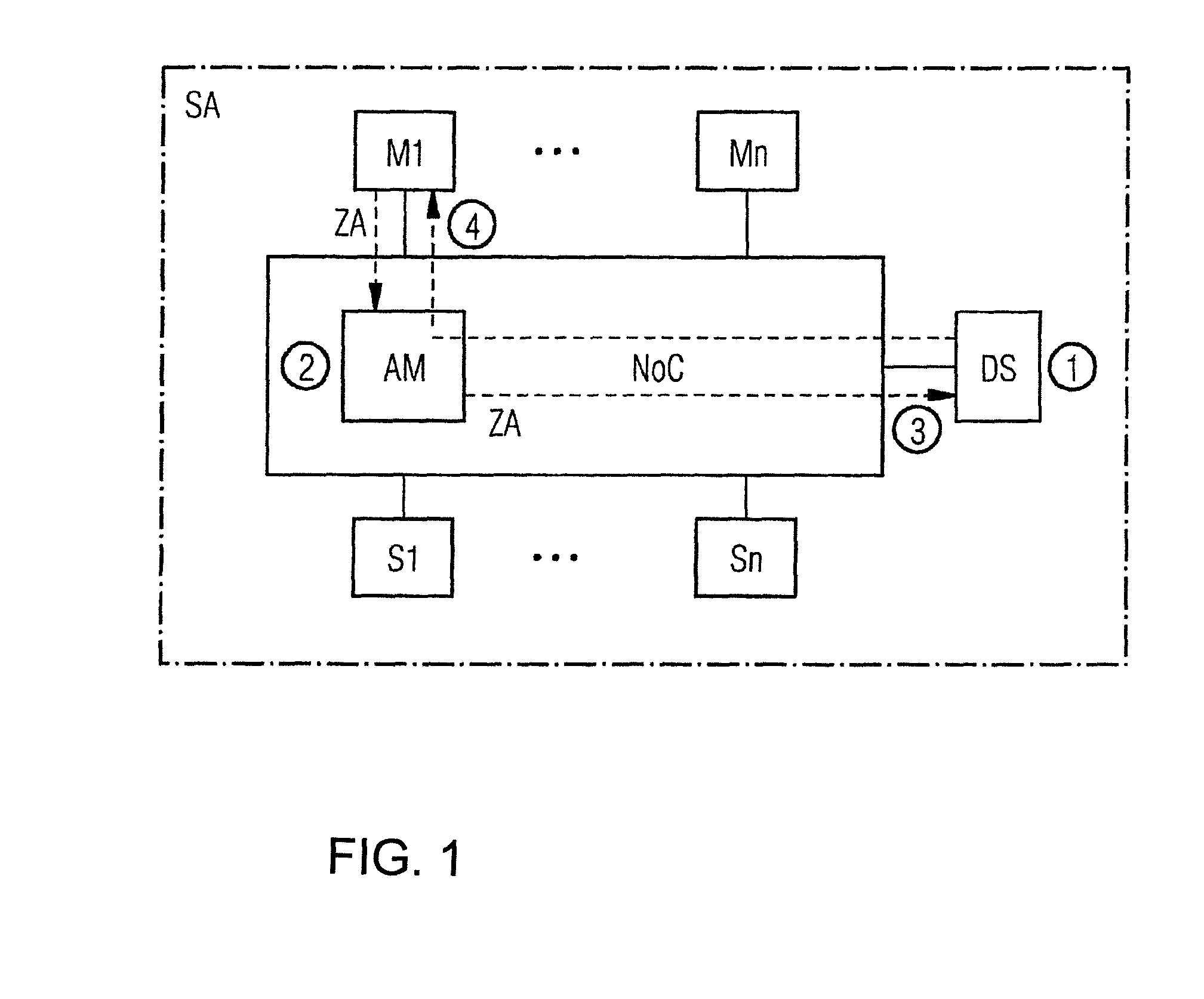
[0030]FIG. 1 shows schematically an exemplary circuit arrangement SA for implementing the method in accordance with the invention for protecting an integrated electronic circuit against scanning of an address space of this circuit. The circuit arrangement in accordance with the invention comprises at least one master device M1 to Mn, e.g., devices such as processors, controllers, or special processors, and at least one slave device S1 to Sn, e.g., devices such as memory devices, or input / output devices. In addition, the circuit arrangement SA in accordance with the invention comprises a bus system NoC, which is, for example, a standard product available on the market for bus systems, i.e., a network-on-chip bus system.

[0031]The at least one master device M1 to Mn is connected to the at least one slave device S1 to Sn via the bus system NoC. The exemplary circuit arrangement SA shown in FIG. 1 comprises a plurality of master devices M1 to Mn and a plurality of slave devices S1 to Sn....


PUM


Abstract

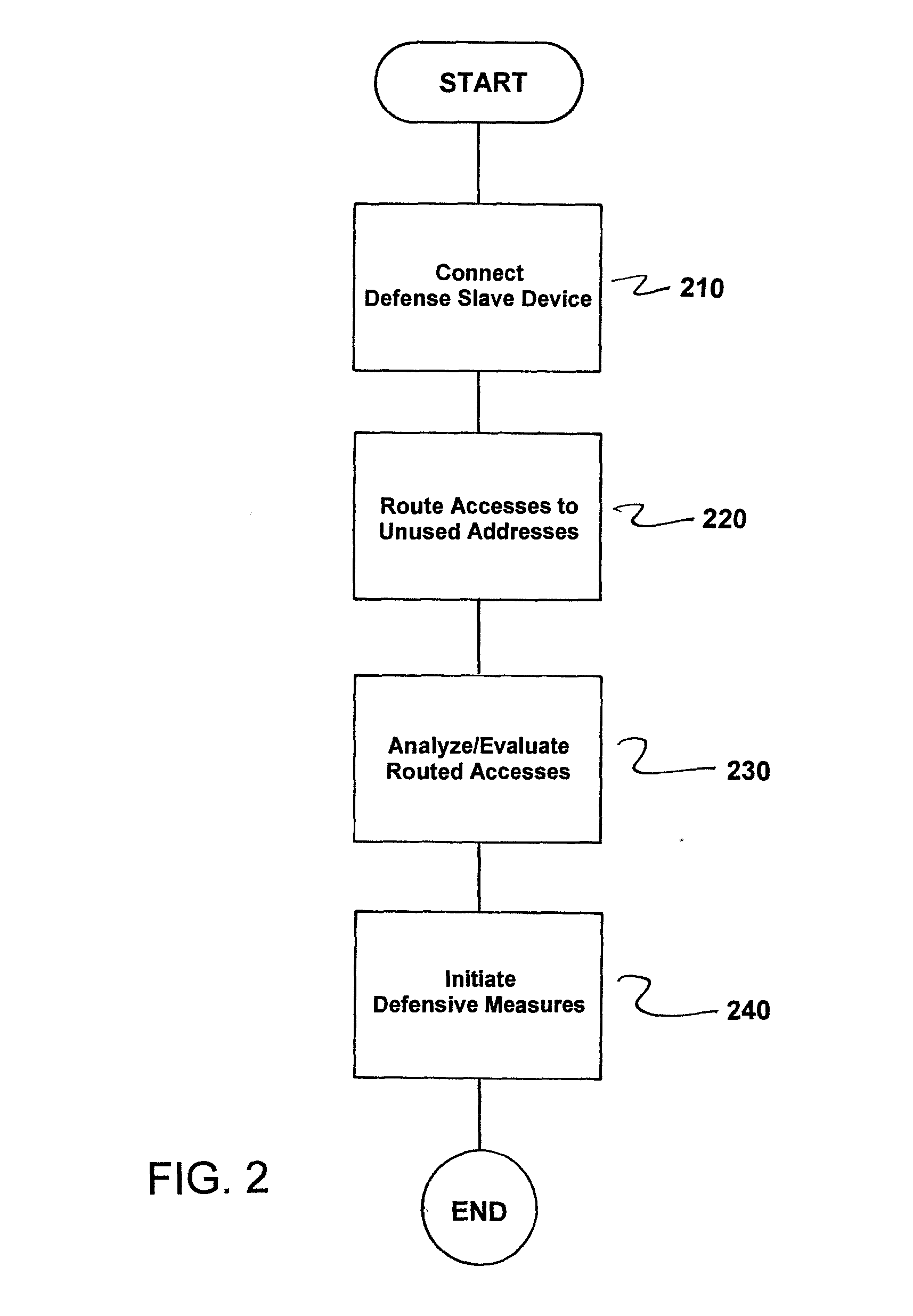
A circuit arrangement and method for securing an integrated electronic circuit against scans of an address space, wherein the circuit arrangement has at least one master unit and at least one slave unit interconnected via a bus system for access of the master unit to the slave unit, and addresses are used from an address space that is allocated and used in accordance with functionalities of the integrated electronic circuit, where a defense slave unit is connected to the bus system, access to unused address regions of the address space are forwarded to the defense slave unit, the access is analyzed and evaluated by the defense slave unit and depending on an analysis result and the respective access type, defensive measures are triggered, such that address space scans are interrupted or a potential scan result is rendered useless in a simple manner.

Description

CROSS-REFERENCE TO RELATED APPLICATIONS[0001]This is a U.S. national stage of application No. PCT / EP2014 / 065391 filed 17 Jul. 2014. Priority is claimed on German Application No. 10 2013 216 699.0 filed 22 Aug. 2013, the content of which is incorporated herein by reference in its entirety.BACKGROUND OF THE INVENTION[0002]1. Field of the Invention[0003]The present invention relates generally to the field of electronic and logic circuits, in particular integrated electronic circuits such as application-specific integrated circuits (ASICs) or field programmable gate arrays (FPGAs) and, more specifically, to a method and circuit arrangement for protecting integrated circuits, such as ASICs, FPGAs, particularly in the form of system-on-chip devices, against scanning of an address space, which integrated circuit comprises at least one master device, at least one slave device and a bus system for a connection between master device and slave device where accesses between the master device an...

Claims


Application Information

Patent Timeline
Patent Type & Authority Applications(United States)
IPC IPC(8): G06F21/76G06F13/42G06F13/364G06F21/75G06F21/85
CPCG06F21/76G06F21/75G06F13/4282G06F13/364G06F21/85
Inventor EPPENSTEINER, FRIEDRICHGHAMESHLU, MAJIDTAUCHER, HERBERT
Owner SIEMENS AG OESTERR
Learn More