Power conversion device

a power conversion device and power conversion technology, applied in the direction of solid-state devices, semiconductor devices, electrical apparatus construction details, etc., can solve the problems of increasing current, voltage, sw speed of sw elements, and reducing the radiation performance of sw elements. , the effect of high radiation performance of sw elements

Active Publication Date: 2016-07-21
DENSO CORP
View PDF5 Cites 9 Cited by
  • Summary
  • Abstract
  • Description
  • Claims
  • Application Information

AI Technical Summary

Benefits of technology

[0032]According to an eleventh aspect of the present disclosure, in order to ensure satisfactory radiation performance of the SW elements as described above, the power conversion device adopts double-sided heat-sinking element modules. Herein, the power conversion device may be configured in such a manner that the element modules of the two SW elements are disposed between water-cooling coolers via an insulating layer. Hence, heat generated in the SW elements (heat generated in the capacitor element and the resistor when the snubber circuit is connected) is transferred to the water-cooling coolers from the heat sinks exposed to the outer surfaces of the respective element modules via the insulating layer. Consequently, a high cooling effect can be exerted.
[0033]As has been described, the power conversion device described above is a power conversion device capable of achieving three requirements to restrict a surge voltage, ensure high radiation performance of SW elements, and restrict ringing at the same time. Hence, according to a twelfth aspect of the present disclosure, the power conversion device described above can be employed in a vehicle for which a power conversion device having high power density and a small power loss is required and restriction of a surge voltage becomes a problem when a current, a voltage, and a SW speed of the SW elements are increased.

Problems solved by technology

Accordingly, restriction of a surge voltage becomes a problem as a current, a voltage, and a SW speed of the SW elements are increased.

Method used


Image

  • Power conversion device
  • Power conversion device
  • Power conversion device

Examples


Embodiment Construction

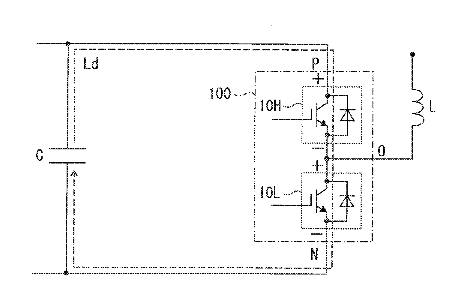
[0064]A power conversion device of the present disclosure includes two serially-connected SW elements of an upper arm and a lower arm and supplies power to a load from a connection point of the two SW elements by converting a voltage and a current from a DC power supply.

[0065]Hereinafter, embodiments of the power conversion device of the present disclosure will be described according to the drawings.

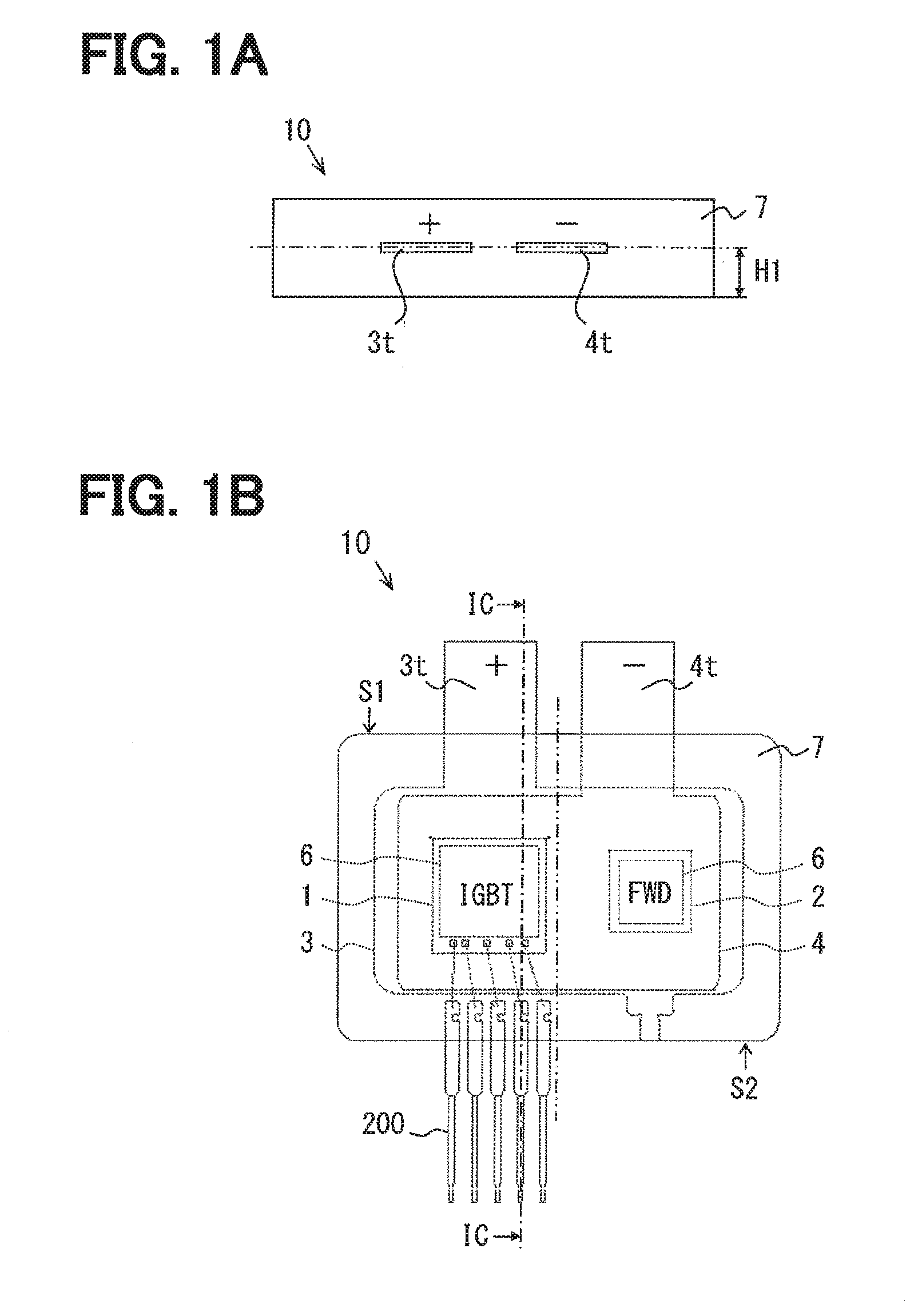
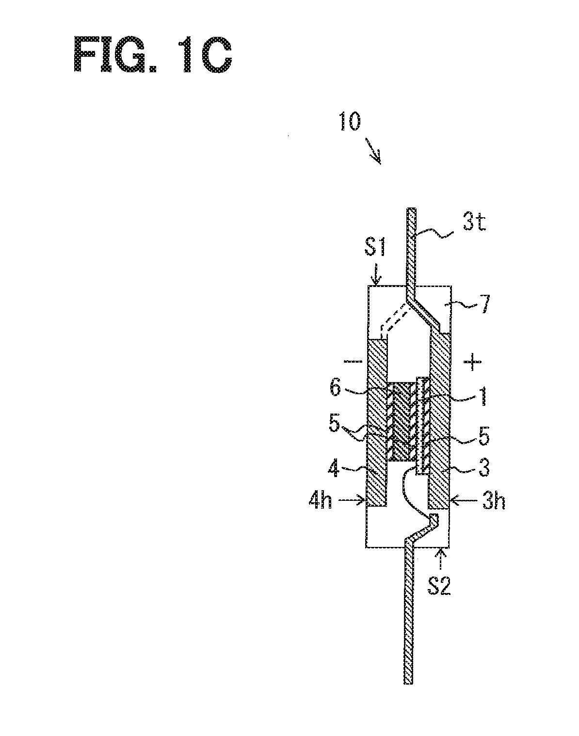
[0066]FIG. 1A through FIG. 1C are views showing an example of an element module of a SW element used in the power conversion device of the present disclosure. FIG. 1A is a front view of an element module 10. FIG. 1B is a bottom view of the element module 10 to see through an interior. FIG. 1C is a sectional view taken along the alternate long and short dash line IC-IC of FIG. 1B.

[0067]FIG. 2A through FIG. 2C show an example of the power conversion device of the present disclosure using the SW element (element module 10) of FIG. 1A through FIG. 1C. FIG. 2A is a circuit diagram showing an ...


PUM


Abstract

A power conversion device is capable of achieving three requirements to restrict a surge voltage, ensure high radiation performance of SW elements, and restrict ringing at the same time. In a power conversion device, element modules of two SW elements are stacked in a thickness direction via an insulating layer in such a manner that lateral surfaces are aligned parallel to each other in a same orientation, and a positive terminal of one SW element and a negative terminal of the other SW element are disposed so as to overlap each other in the thickness direction.

Description

CROSS REFERENCE TO RELATED APPLICATION[0001]This application is based on Japanese Patent Application No. 2013-187550 filed on Sep. 10, 2013, the disclosure of which is incorporated herein by reference.TECHNICAL FIELD[0002]The present disclosure relates to a power conversion device which includes two serially-connected switching elements (hereinafter, referred to as the SW elements) of an upper arm and a lower arm and supplies power to a load from a connection point of the two SW elements by converting a voltage and a current from a DC power supply.BACKGROUND ART[0003]A power conversion device which includes two serially-connected SW elements of an upper arm and a lower arm and supplies power to a load by converting a voltage and a current from a DC power supply is disclosed, for example, in JP2005-287267A (Patent Literature 1).[0004]A power conversion device employed in a vehicle is required to have high power density (compact size and large current) and a small power loss. To this ...

Claims


Application Information

Patent Timeline
Patent Type & Authority Applications(United States)
IPC IPC(8): H02M1/34H05K7/20H02M7/537H02M7/00
CPCH02M1/34H02M7/003H02M2001/348H02M7/537H05K7/209H01L2224/40137H01L2224/48247H01L2924/181H01L2224/05554H01L2224/371H01L2224/37147H01L2924/13055H01L2224/0603H02M1/348H01L2924/00012H01L2924/00
Inventor ISHINO, HIROSHIJINSEI, YOUSUKEIKEGAME, ATSUSHI
Owner DENSO CORP
Why Eureka
Try Eureka