Semiconductor equipment and method of manufacturing the same

Inactive Publication Date: 2011-10-20
PANASONIC CORP
View PDF5 Cites 7 Cited by
  • Summary
  • Abstract
  • Description
  • Claims
  • Application Information

AI Technical Summary

Benefits of technology

[0053]According to this configuration, a semiconductor equipment having the above-described characteristics can be easily manufactured.
[0054]The pre

Problems solved by technology

As a result, since the thermal conductivity of the packaging material is low, the heat of the semiconductor chip surface is not easily transmitted to the working flu

Method used


Image

  • Semiconductor equipment and method of manufacturing the same
  • Semiconductor equipment and method of manufacturing the same
  • Semiconductor equipment and method of manufacturing the same

Examples


embodiment 1

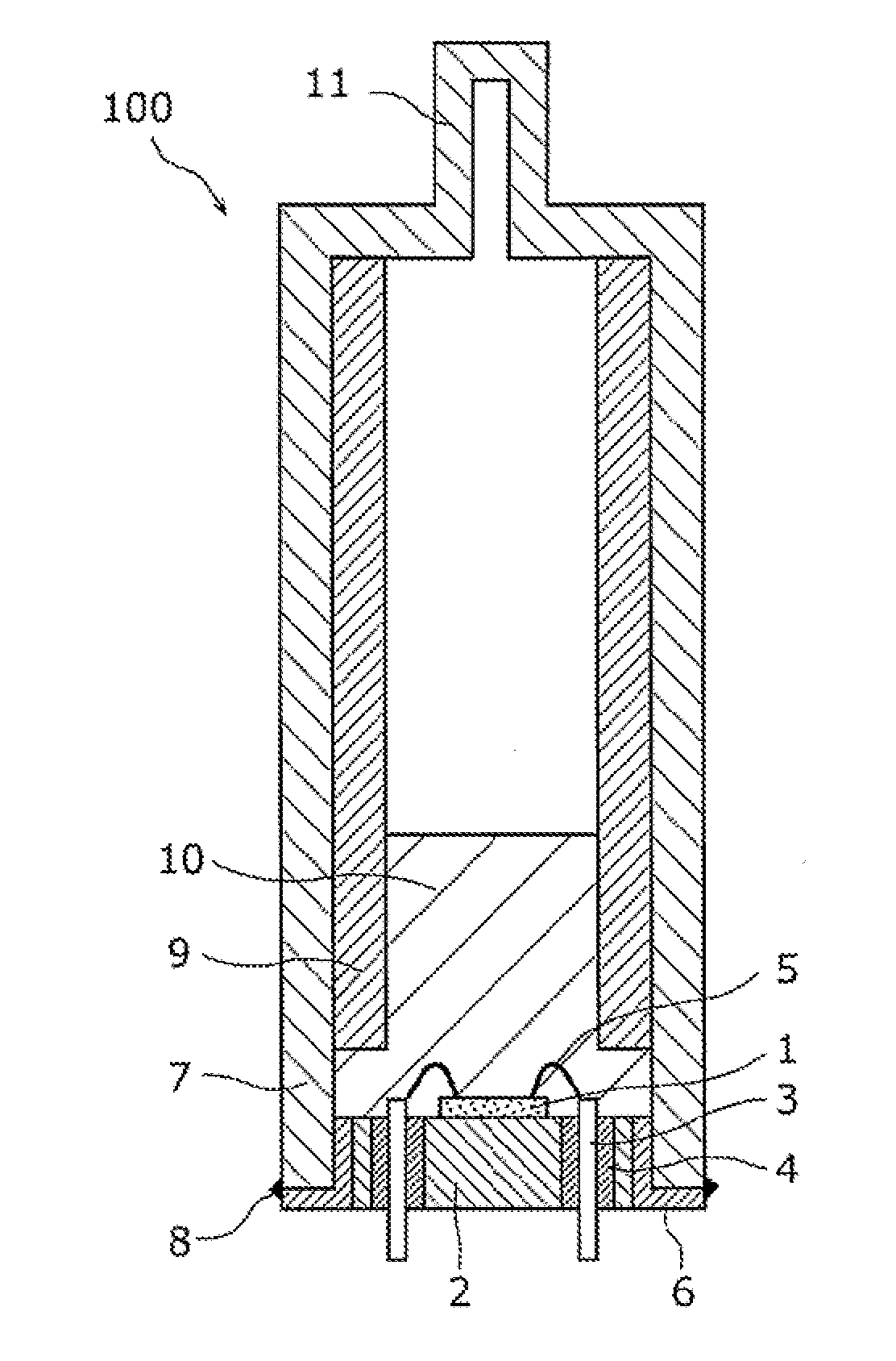
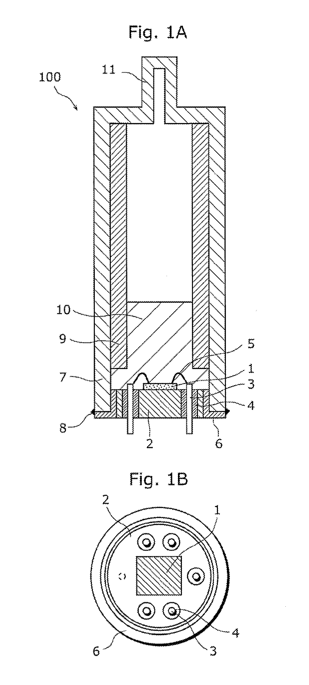
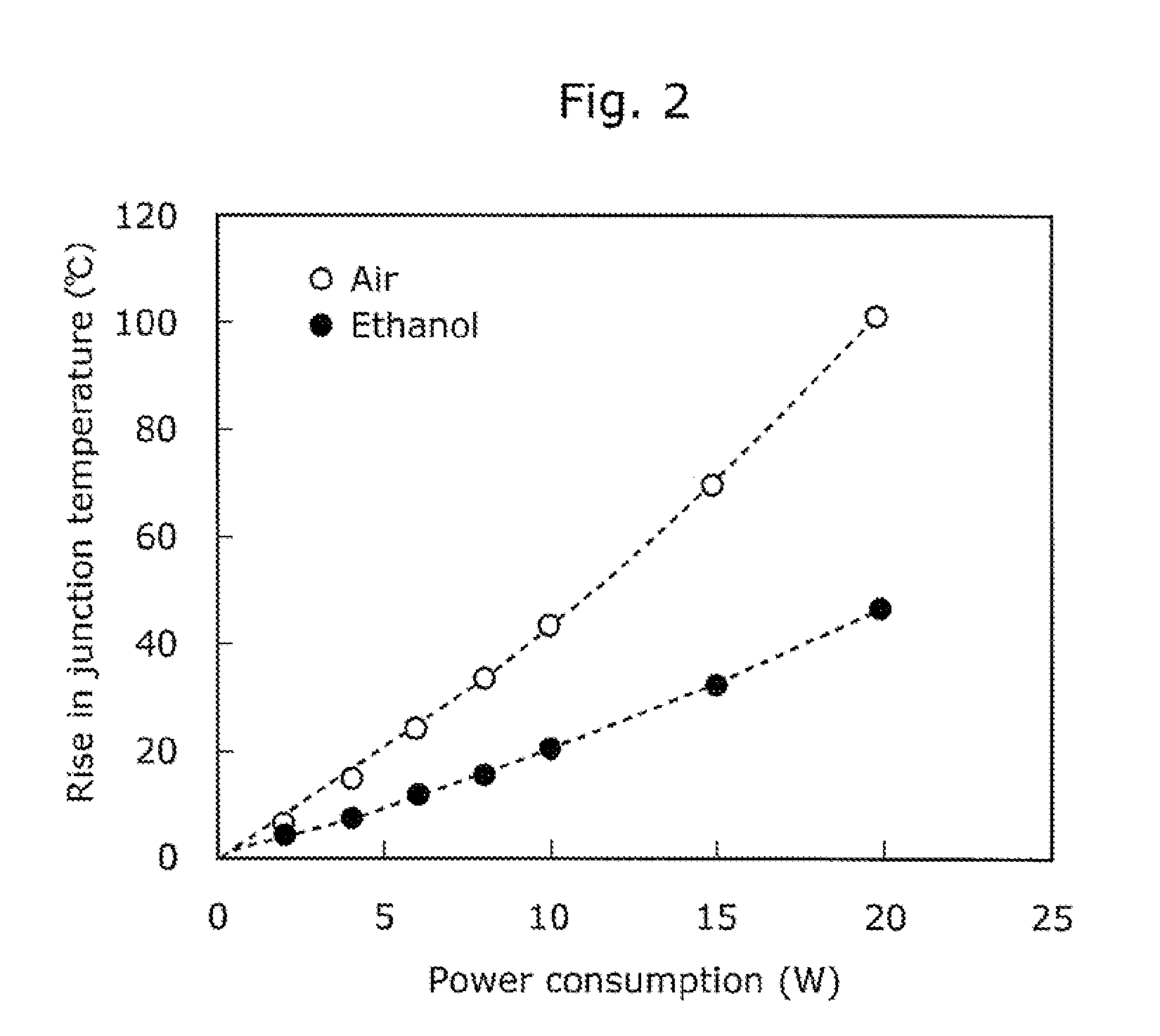
[0088]FIG. 1A is a cross-sectional view of a semiconductor equipment according to Embodiment 1 of the present invention. Furthermore, FIG. 1B is a bottom view of a stem of the semiconductor equipment shown in FIG. 1A. FIG. 2 is a graph showing the relationship between the rise in junction temperature and power consumption, in the semiconductor equipment according to the present embodiment. FIG. 3 is a graph showing the relationship between thermal resistance and pulse width, in the semiconductor equipment according to the present embodiment. FIG. 4A to FIG. 4F are diagrams for describing a method of manufacturing the semiconductor equipment according to the present embodiment. FIG. 5 is a graph showing the relationship between the latent heat and boiling point of the working fluid, in the semiconductor equipment according to the present embodiment. FIG. 6 is a graph showing the relationship between the latent heat of the working fluid and insulation breakdown voltage, in the semicon...

embodiment 2

[0157]Next, Embodiment 2 of the semiconductor equipment according to the present invention shall be described using FIG. 9 and FIG. 10A to FIG. 10C. FIG. 9 and FIG. 10A to FIG. 10C are cross-sectional views of the semiconductor equipment according to the present embodiment.

[0158]A semiconductor equipment 120 according to the present embodiment has the same fundamental configuration as the semiconductor equipment 100 according to Embodiment 1 of the present invention. Therefore, constituent elements in FIG. 9 and FIG. 10A to FIG. 10C which are the same as the constituent elements shown in FIG. 1A are assigned the same numerical references, and detailed explanation thereof shall be omitted or simplified. Furthermore, constituent elements other than those shown in FIG. 9 and FIG. 10A to FIG. 10C are the same as those in Embodiment 1.

[0159]The semiconductor equipment 120 according to the present embodiment is different from Embodiment 1 in that a concave recess is formed as a chip place...

embodiment 3

[0167]Next, Embodiment 3 of a semiconductor equipment according to the present invention shall be described using to FIG. 11 and FIG. 12. FIG. 11 is a cross-sectional view of a semiconductor equipment according to the present embodiment. FIG. 12 is a graph showing the relationship between thermal resistance and pulse width, in the semiconductor equipment.

[0168]A semiconductor equipment 150 according to the present embodiment has the same fundamental configuration as the semiconductor equipment 100 according to Embodiment 1 of the present invention. Therefore, constituent elements in FIG. 11 which are the same as the constituent elements shown in FIG. 1A are assigned the same numerical references, and detailed explanation thereof shall be omitted or simplified. Furthermore, constituent elements other than those shown in FIG. 11 are the same as those in Embodiment 1.

[0169]Instead of a configuration in which the semiconductor chip is directly mounted onto the stem, as a semiconductor d...


PUM


Abstract

To provide a semiconductor equipment having high heat-transfer effect and breakdown voltage, and a method of manufacturing the same. The semiconductor equipment includes: a sealed container; a stem connected to the sealed container via a stem peripheral portion; and a semiconductor chip mounted on a top surface of the stem, inside the sealed container. The semiconductor chip is electrically connected to a lead provided to the stem, the stem peripheral portion, which is of a material that is different from the material of stem and the same as the material of the sealed container, is bonded along a periphery of the stem, and the sealed container is filled with a working fluid including at least one of ethanol, a perfluorocarbon, and a fluoroether.

Description

CROSS REFERENCE TO RELATED APPLICATION[0001]This is a continuation application of PCT application No. PCT / JP2010 / 005515 filed on Sep. 9, 2010, designating the United States of America.BACKGROUND OF THE INVENTION[0002](1) Field of the Invention[0003]The present invention relates to a semiconductor equipment which includes a semiconductor chip inside a heat pipe, and to a method of manufacturing the semiconductor equipment.[0004](2) Description of the Related Art[0005]As a material for semiconductor devices, recent years have seen active research and development being carried out on wide bandgap semiconductors such as nitride semiconductors, represented by gallium nitride (GaN), and silicon carbide (SiC).[0006]Wide bandgap semiconductors are characterized in that dielectric breakdown voltage is one digit higher compared to that of Si, and that the on-resistance of a semiconductor device decreases. In particular, since a nitride semiconductor material such as gallium nitride (GaN), tog...

Claims


Application Information

Patent Timeline
IPC IPC(8): H01L23/44H01L21/54
CPCH01L21/50H01L21/54H01L23/045H01L23/10H01L23/427H01L2924/01322H01L2224/45124H01L2924/10253H01L2924/13091H01L2224/48H01L2924/00H01L2224/45014H01L2224/45144H01L2224/73265H01L2924/00014H01L2924/181H01L2924/00012H01L2924/206
Inventor OTSUKA, NOBUYUKIYANAGIHARA, MANABUNAGAI, SHUICHIUEDA, DAISUKE
Owner PANASONIC CORP
Why Eureka
Try Eureka