

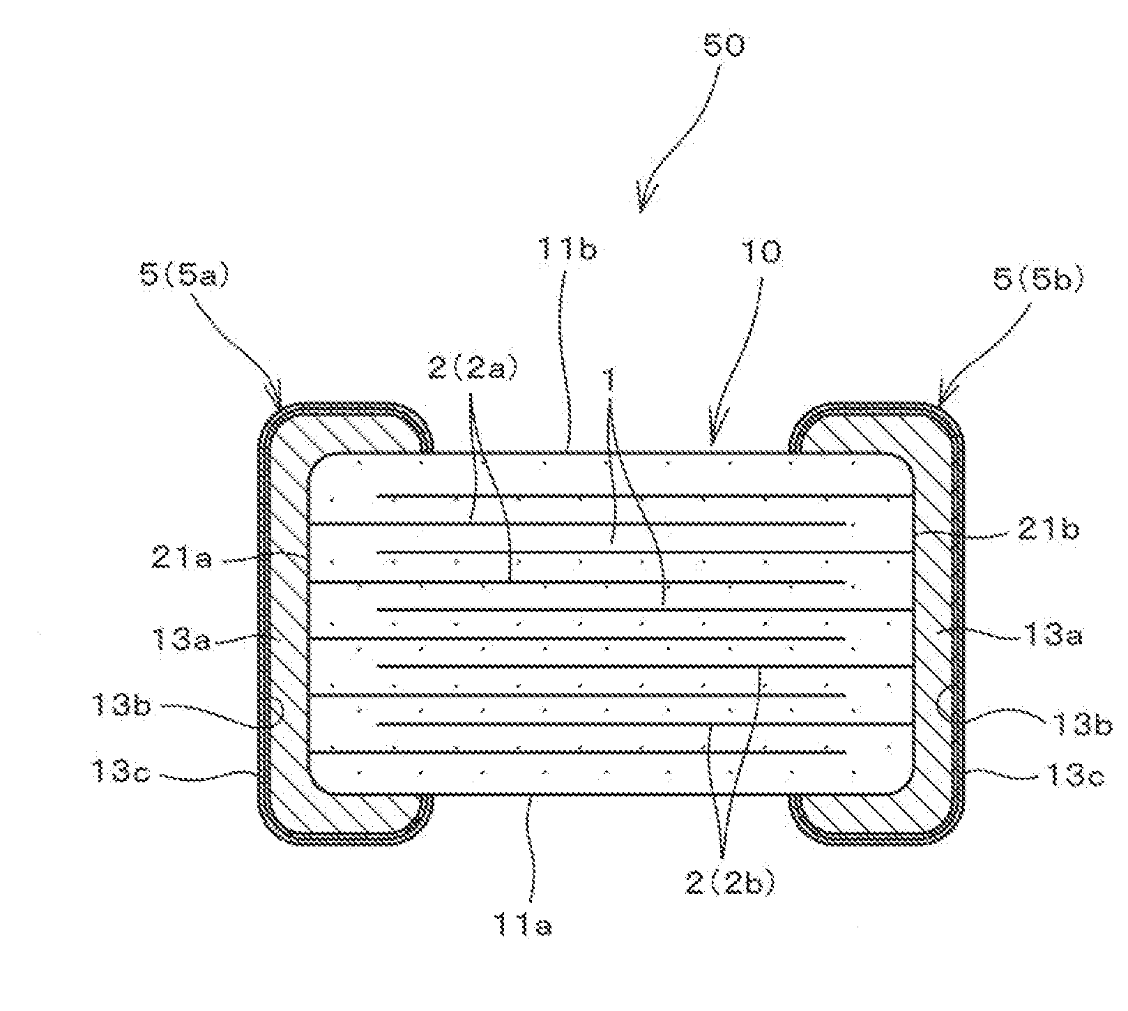
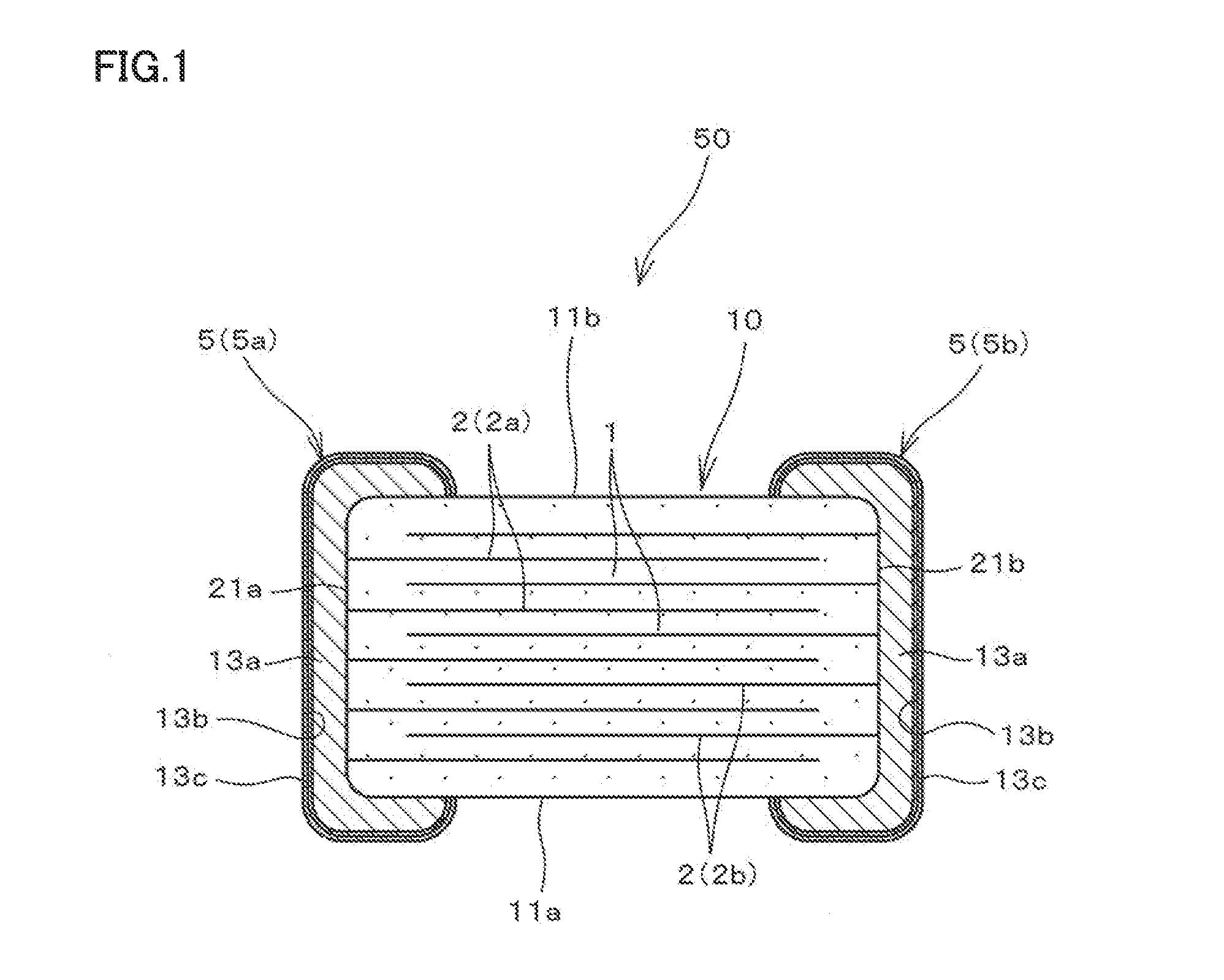
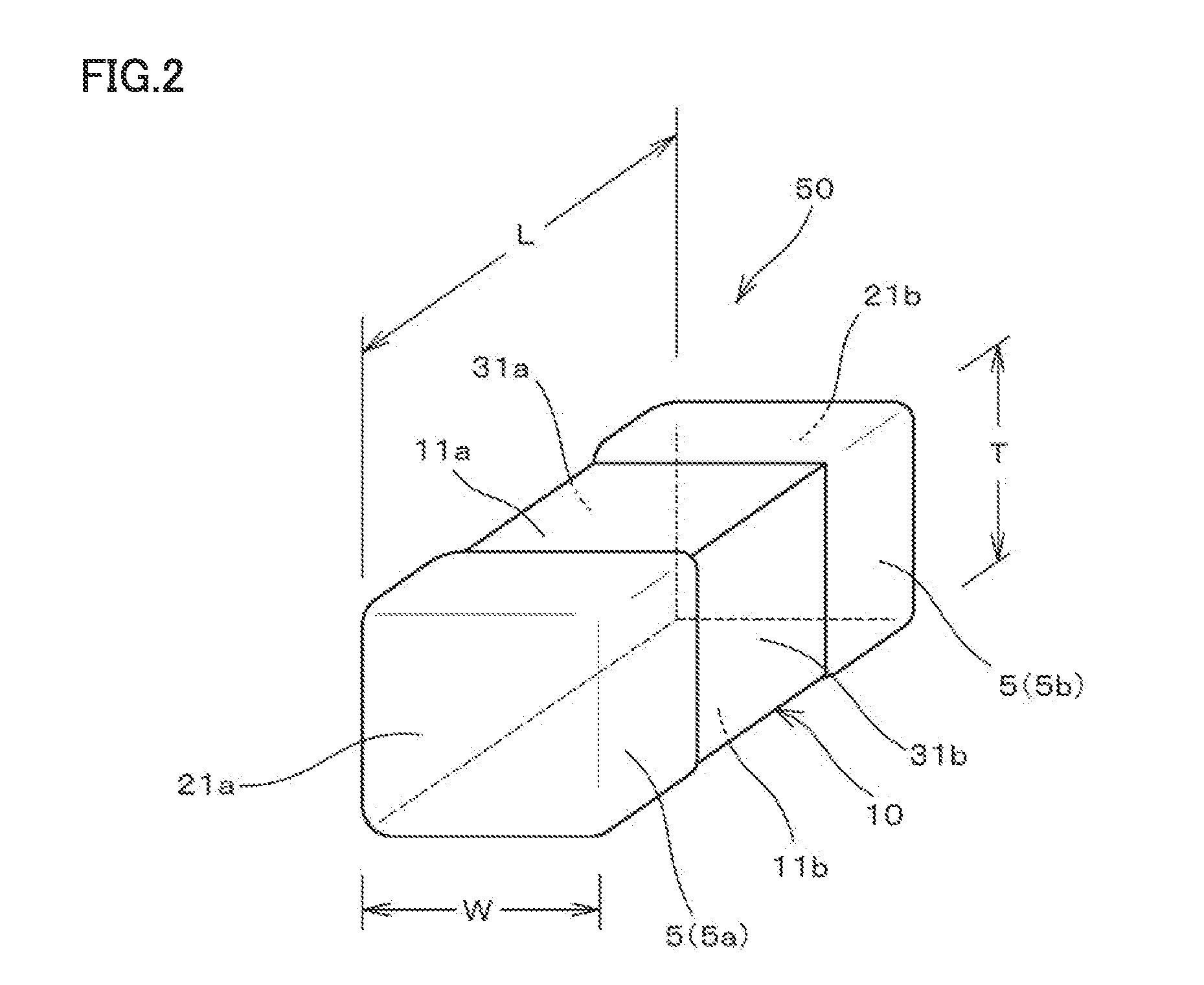
Multilayer ceramic capacitor and method for manufacturing the same
- Summary
- Abstract
- Description
- Claims
- Application Information
AI Technical Summary
Benefits of technology
Problems solved by technology
Method used
Image

Examples
experimental example 1
[0081]In order to confirm the significance of the multilayer ceramic capacitor according to this preferred embodiment, samples (multilayer ceramic capacitors) of Sample Nos. 1 to 10 shown in Table 1 were produced using a conductive paste obtained by adding Sn to a conductive paste containing a Cu powder as a conductive material.
[0082]Note that a detailed specification of the conductive paste was set as follows.
[0083]Solids content: 25 vol %
[0084]Ratio of the Cu powder in the solids content: 70 vol %
[0085]Ratio of a glass in the solids content: 25 vol %
[0086]Ratio of Sn in the solids content: 5 vol %
[0087]Particle size of the Cu powder: 3 μm
[0088]Particle size of the glass: 2 μm
[0089]Composition of the glass: BaO—SrO—B2O3—SiO2-based glass frit (glass with glass frit containing 10 to 50 wt % of BaO, 3 to 30 wt % of B2O3, and 3 to 30 wt % of SiO2 in terms of oxides)
[0090]When producing the samples of Sample Nos. 1 to 10 shown in Table 1, this conductive paste was applied to first end s...
experimental example 2
[0117]Samples of Sample Nos. 11 to 15 shown in Table 2 were produced in the same manner as that for the samples according to Experimental Example 1 above (samples shown in Table 1), except that the thickness of the external electrode main body was set to about 40 μm, and the thickness of the mutual diffusion layer on the external electrode was set to about 10% of the thickness of the external electrode main body, and that the thickness of the mutual diffusion layer on the internal electrode was varied in the range from about 0.2 μm to about 7 μm.
[0118]Each of the produced samples was then subjected to a test for examining the number of cracks and the zero-Ω discharge test.
[0119]Note that the number of cracks was examined as follows: each sample was polished from surfaces (end surfaces of the ceramic body on which the external electrodes were formed) including the thickness direction and the width direction of the sample (multilayer ceramic capacitor); the polishing was stopped at th...
PUM
| Property | Measurement | Unit |
|---|---|---|
| Temperature | aaaaa | aaaaa |
| Temperature | aaaaa | aaaaa |
| Temperature | aaaaa | aaaaa |
Abstract
Description
Claims
Application Information