Semiconductor device

a technology of mikro-onductors and shields, applied in the field of mikro-onductors, can solve the problems of weak stress applied to the hall elements below, the function of amplifying magnetism the piezoelectric effect cannot be sufficiently inhibited, so as to achieve the effect of preventing stress and low cos

Inactive Publication Date: 2016-09-22
ABLIC INC
View PDF4 Cites 7 Cited by
  • Summary
  • Abstract
  • Description
  • Claims
  • Application Information

AI Technical Summary

Benefits of technology

[0015]According to the one embodiment of the present invention, the slit or the slot is formed in the magnetic material (magnetic flux concentrator), and thus, stress is prevented from being applied as much as possible not only to the Hall elements but also to all elements arranged below the magnetic material such as a transistor, a resistor, and a capacitor, and hence a semiconductor device capable of adjusting stress may be provided at a low cost with ease.

Problems solved by technology

When such a magnetic tape is used, the magnetic tape is bonded onto the semiconductor substrate 11 using an epoxy adhesive 12, and thus, there is a problem in that strong stress is applied to the Hall elements therebelow.
However, the technology disclosed in Japanese Patent No. 5064706 (see FIGS. 7A-7B) has a problem in that a small thickness of a magnetic material (magnetic flux concentrator) lowers the function of amplifying magnetism.
Hence, there is a problem in that generation of an offset voltage and the like due to a piezoelectric effect cannot be sufficiently inhibited.
Further, elements other than the Hall elements are arranged as well below the magnetic material, and thus, change in characteristics thereof due to the stress in a similar way is another problem.

Method used


Image

  • Semiconductor device
  • Semiconductor device
  • Semiconductor device

Examples


Embodiment Construction

[0023]Embodiments of the present invention are described below with reference to the attached drawings.

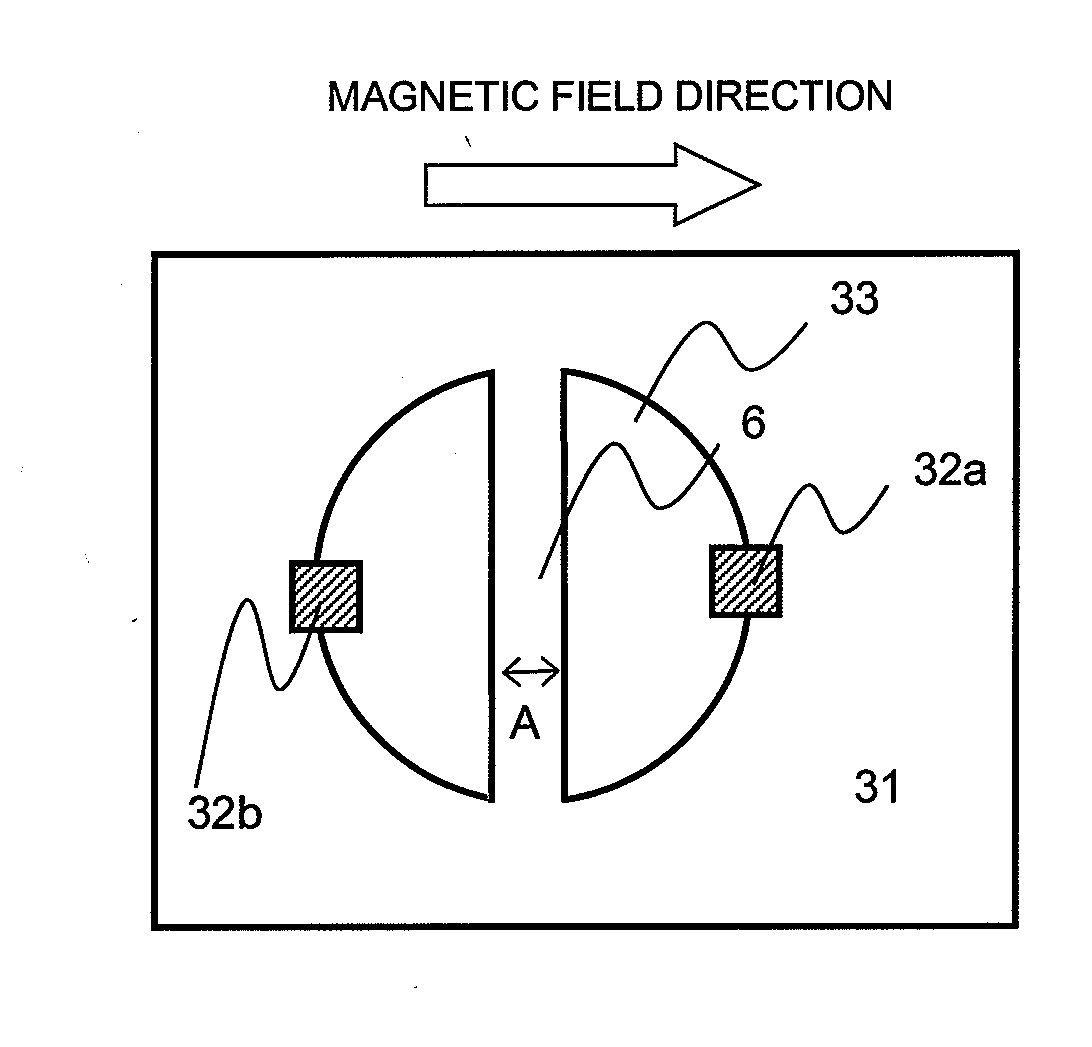
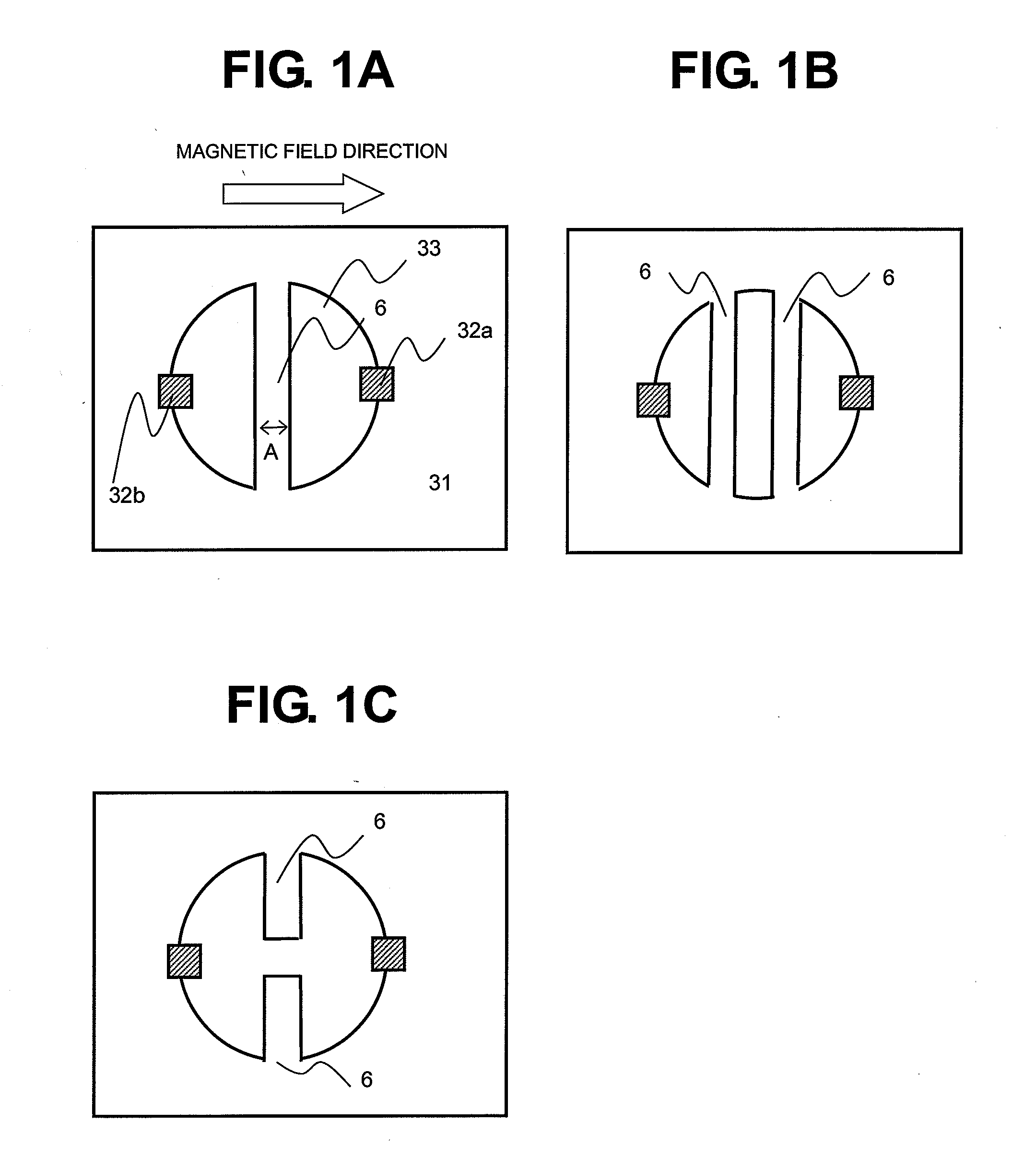
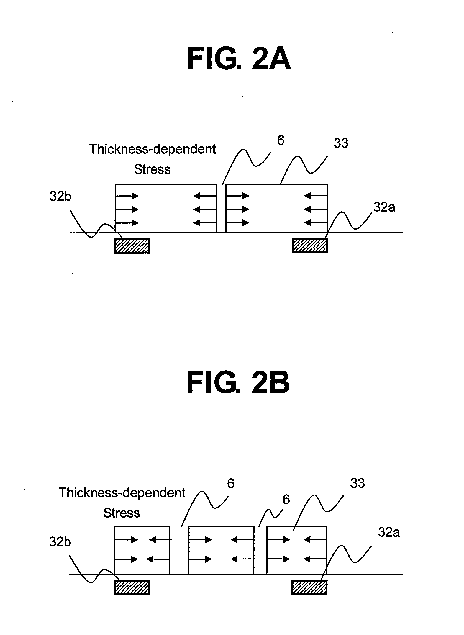
[0024]FIG. 1A, FIG. 1B, and FIG. 1C are plan views for illustrating a magnetic sensor serving as a semiconductor device according to one embodiment of the present invention. Hall elements 32a and 32b are spaced in a surface of a semiconductor substrate 31. A magnetic flux concentrator 33 is arranged above the Hall elements 32a and 32b via a protective film. The magnetic flux concentrator 33 is arranged so that an edge, namely, an outer periphery thereof may be positioned above the Hall elements 32a and 32b. The slit 6 is formed in the magnetic flux concentrator 33. A slit 6 as used herein means a groove formed inward from the outer periphery (edge) of the magnetic flux concentrator 33. The groove pierces the magnetic concentrator 33 from a top surface of the magnetic flux concentrator 33 to a bottom surface thereof.

[0025]The magnetic flux concentrator 33 can be formed by electrolyt...


PUM


Abstract

In a semiconductor device having a magnetic sensor configured to detect a direction of magnetism, stress applied by a magnetic flux concentrator that is a magnetic material is small. The magnetic sensor includes, in combination, Hall elements arranged on a surface of a semiconductor substrate, and a magnetic flux concentrator formed of a magnetic material having the function of amplifying magnetism, the magnetic flux concentrator being arranged on the semiconductor substrate, for at least partly covering each of the Hall elements. A slit or a slot is formed in the magnetic material to inhibit generation of stress applied to the Hall elements.

Description

BACKGROUND OF THE INVENTION[0001]1. Field of the Invention[0002]The present invention relates to a semiconductor device, and more particularly, to a semiconductor device including a sensor configured to detect a direction of magnetism.[0003]2. Description of the Related Art[0004]A magnetic sensor technology has hitherto been known well in which a magnetic material, a magnetic flux concentrator, having a function of amplifying magnetism and a Hall element are combined. For example, in Japanese Patent No. 4936299, there is disclosed a technology relating to a sensor configured to detect a direction of a magnetic field that can detect a vertical magnetic field and a horizontal magnetic field. The sensor includes a magnetic flux concentrator formed on a surface of a semiconductor chip and having a flat shape, and a plurality of Hall elements. These Hall elements are arranged in an end portion region of the magnetic flux concentrator. Such a structure has an effect that magnetism in the ...

Claims


Application Information

Patent Timeline
Patent Type & Authority Applications(United States)
IPC IPC(8): H01L43/04H01L43/06G01R33/00H01L27/22
CPCH01L43/04G01R33/0011H01L43/06H01L27/22G01R33/07H10B61/00H10N59/00H10N52/80H10N52/101G01R33/06G01R15/20G01R15/202G01R33/077G01R21/08H10N52/00
Inventor EBIHARA, MIKA
Owner ABLIC INC
Why Eureka
Try Eureka