One Transistor Active Pixel Sensor with Tunnel FET

a technology of active pixel sensor and transistor, which is applied in the direction of electrical equipment, semiconductor devices, radio frequency controlled devices, etc., can solve problems such as noise related problems

Active Publication Date: 2016-09-29
ECOLE POLYTECHNIQUE FEDERALE DE LAUSANNE (EPFL)
View PDF1 Cites 39 Cited by
  • Summary
  • Abstract
  • Description
  • Claims
  • Application Information

AI Technical Summary

Benefits of technology

[0007]According to one aspect of the present invention, a tunneling field effect transistor for light detection is provided. The tunneling field affect transistor preferably includes a p-type region connected to a source terminal, a n-type region connected to a drain terminal, and an intrinsic region located between the p-type region and the n-type region to form a P-I junction or an N-I junction with the n-type region or the p-type region, respectively. Moreover, the tunneling field effect transistor preferably further includes a first insulating layer and a first gate electrode, the first gate electrode covering a portion of the intrinsic region on one side, the first gate configured for applying a gate bias voltage for band-to-band tunneling, and a second insulating layer and a second gate electrode, the second insulating layer and the second gate electrode covering an entire other side of the intrinsic region opposite to the one side, the second gate electrode configured for generating a potential well in the intrinsic region, and an area of the intrinsic region that is not covered by the first gate electrode forms a non-gated intrinsic area configured for the light absorption.
[0008]According to another aspect of the present invention, a method for operating a tunnel field effect transistor for detecting light is provided. Preferably, the tunnel field effect transistor including a source p-type region connected to a source terminal, a drain n-type region connected to a drain terminal, an intrinsic region located between the p-type region and the n-type region to form a P-I junction or a N-I junction with the source n-type region or the drain p-type region, respectively, a first insulating layer and a first gate electrode, the first gate electrode covering a portion of the intrinsic region on one side, and a second insulating layer and a second gate electrode covering an entire other side of the intrinsic region opposite to the one side, an area of the intrinsic region that is not covered by the first gate electrode forming a non-gated intrinsic area for light absorption. In addition, preferably, the method includes the steps of biasing the second gate electrode to remove a potential well in the intrinsic region for removing charges from the intrinsic region, applying a voltage to the second gate electrode to form the potential well in the intrinsic region while simultaneously exposing the non-gated intrinsic area to light to accumulate a charge in the non-gated intrinsic area, and reading out the charge from the non-gated intrinsic area via the drain terminal by generating band-to-band tunneling with a voltage applied to the first gate electrode.

Problems solved by technology

However, the proximity between the circuitry and the active area with the pixels where light absorption takes place in a CMOS sensor may induce noise related problems.

Method used


Image

  • One Transistor Active Pixel Sensor with Tunnel FET
  • One Transistor Active Pixel Sensor with Tunnel FET
  • One Transistor Active Pixel Sensor with Tunnel FET

Examples


Embodiment Construction

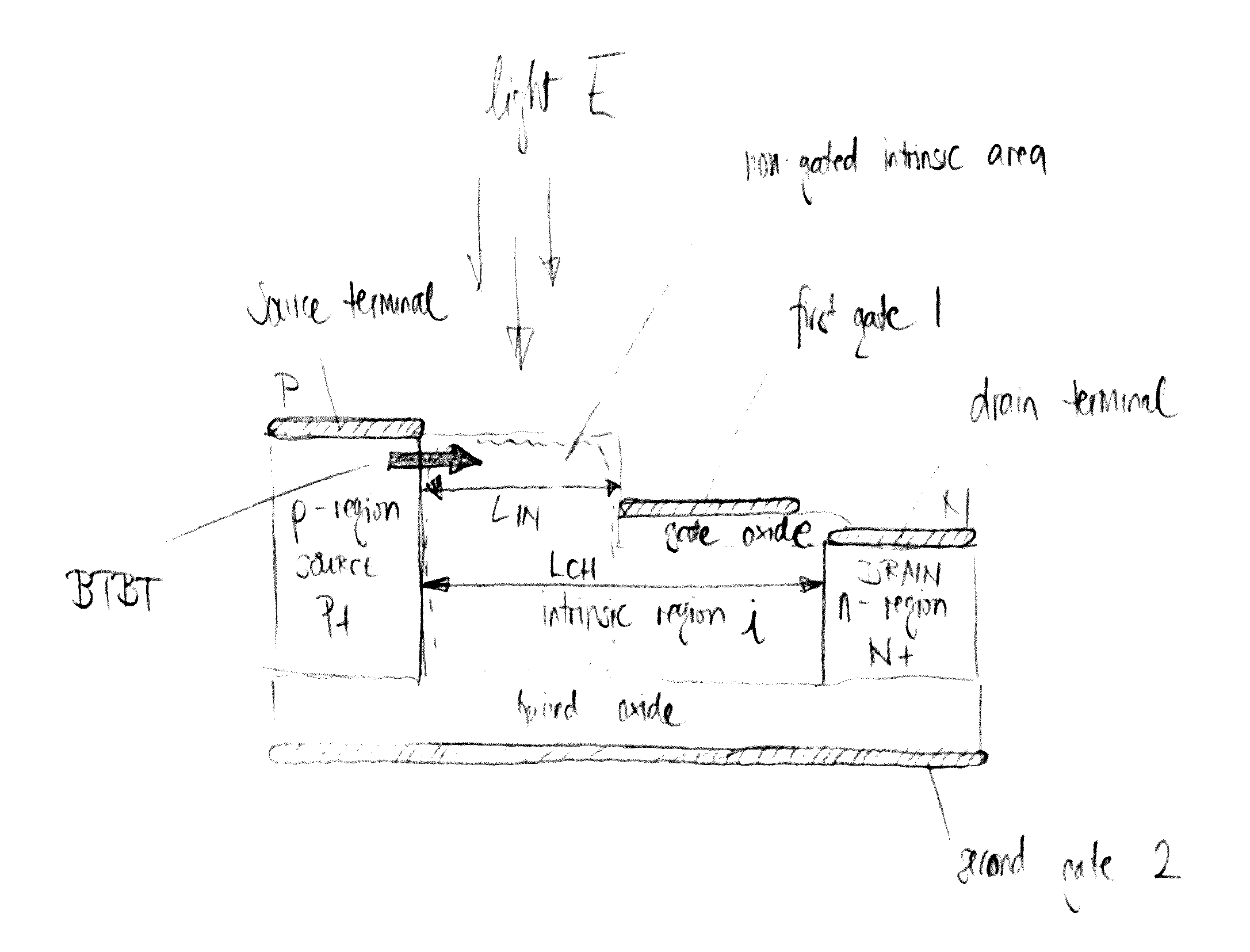
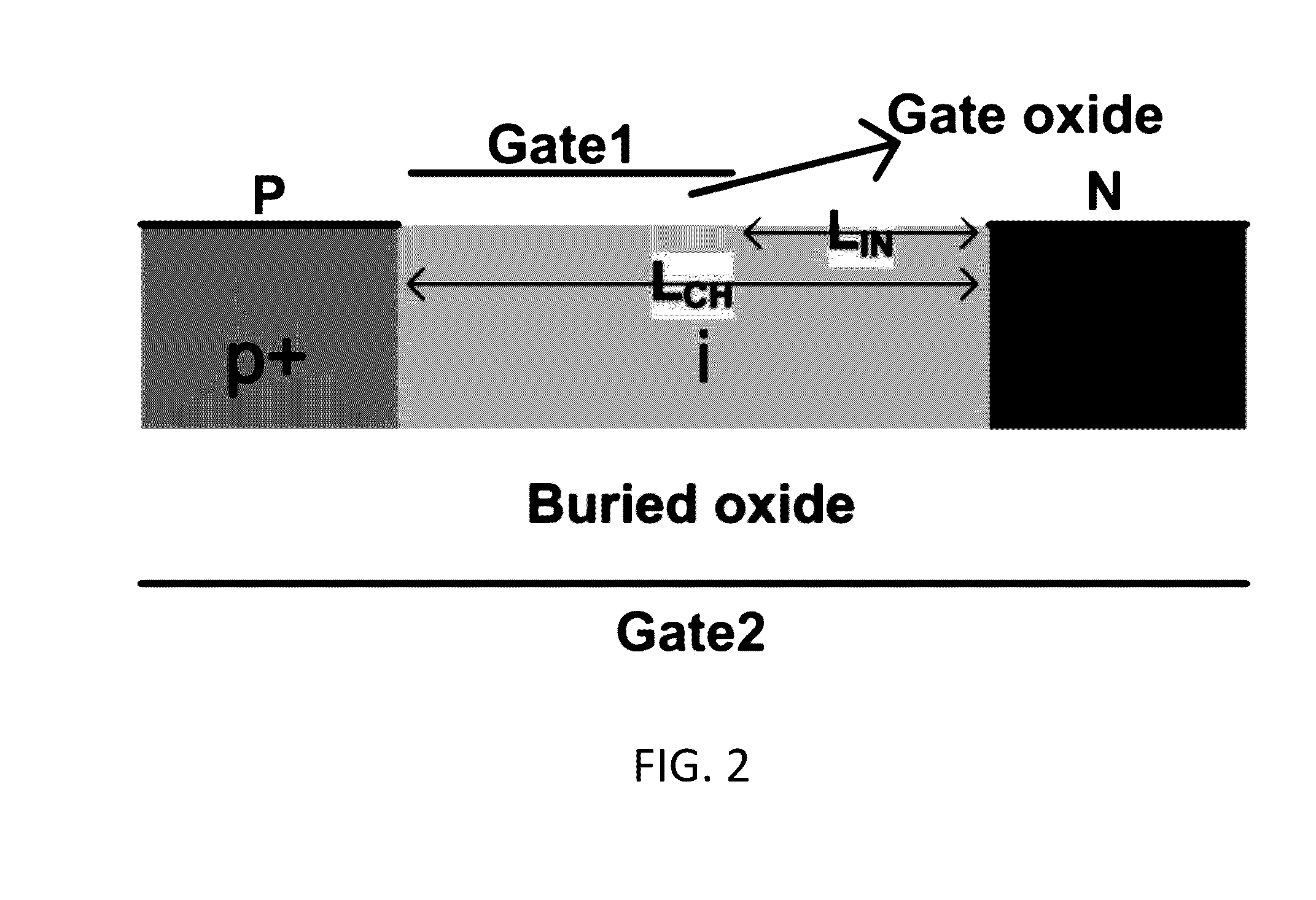
[0022]FIG. 2 shows one aspect of the present invention, depicting a schematic cross-sectional view of a device for sensing light, made by a tunnel field effect transistor (FET) by using a double gate (DG) tunnel FET (TFET), including a source terminal P, a p-doped region P+, a n-doped drain N+, a drain terminal N, an intrinsic region or channel i located between the p-region and the n-region, and a first gate 1 partially overlapping the intrinsic region i arranged on top of the intrinsic region i and a first insulating layer as a gate oxide located between the intrinsic region and the first gate 1. Source terminal P can be a conductive layer such as a metal layer serving as an electrode deposited onto the p-region, and drain terminal N can be a conductive layer such as a metal layer serving as an electrode deposited onto the n-region. Moreover, the DG-TFET device further includes a second insulation layer as a buried oxide arranged below the p-region, the intrinsic region i, and n-r...


PUM


Abstract

A tunneling field effect transistor for light detection, including a p-type region connected to a source terminal, a n-type region connected to a drain terminal, an intrinsic region located between the p-type region and the n-type region to form a P-I junction or an N-I junction with the n-type region or the p-type region, respectively, a first insulating layer and a first gate electrode, the first gate electrode covering a portion of the intrinsic region on one side, and a second insulating layer and a second gate electrode, the second insulating layer and the second gate electrode covering an entire other side of the intrinsic region opposite to the one side, wherein an area of the intrinsic region that is not covered by the first gate electrode forms a non-gated intrinsic area configured for light absorption.

Description

CROSS-REFERENCE TO RELATED APPLICATIONS[0001]The present application claims priority to the Provisional Application with the Ser. No. 62 / 139,095 that was filed on Mar. 27, 2015, the entire contents thereof being herewith incorporated by reference.FIELD OF THE INVENTION[0002]The present invention relates to the field of tunneling devices and solid state optical sensors, and a novel method of using a tunnel field effect transistor (TFET) for light sensing, for example image sensors.DISCUSSION OF THE BACKGROUND ART[0003]Currently, there are two main technologies that are used for image sensing and light detection in a camera: pixels based on the charge-coupled devices (CCD) and complementary metal-oxide semiconductor (CMOS) based active pixel sensors (APS). Both technologies transduce light into an electrical output signal in two steps: first converting the received amount of light into a corresponding number of electrons via photoelectric effect observed in semiconductors, and second,...

Claims


Application Information

Patent Timeline
Patent Type & Authority Applications(United States)
IPC IPC(8): H01L27/146H01L29/78
CPCH01L27/14616H01L27/14649H01L29/7831H01L29/7391
Inventor IONESCU, MIHAI ADRIANDAGTEKIN, NILAY
Owner ECOLE POLYTECHNIQUE FEDERALE DE LAUSANNE (EPFL)
Why Eureka
Try Eureka