Array Substrate, Display Panel and Display Device

a display panel and substrate technology, applied in the field of touch display technologies, can solve the problems of low productivity, large thickness, high cost, etc., and achieve the effect of high touch operation accuracy

Inactive Publication Date: 2016-10-06
SHANGHAI TIANMA MICRO ELECTRONICS CO LTD +1
View PDF4 Cites 15 Cited by
  • Summary
  • Abstract
  • Description
  • Claims
  • Application Information

AI Technical Summary

Benefits of technology

[0013]It can be seen from the above description that, in the technical solutions according to the disclosure, the touch lines are implemented as wirings including multiple line conductive portions and multiple connectors, the line conductive portions of the touch lines are located in the same layer with the gate lines, and two adjacent line conductive portions are electrically connected through the via hole. Therefore, the distance between the conductive layer where the line conductive portions are located and the conductive layer where the touch electrodes are located may be increased, and the coupling capacitance between the line conductive portions and the touch electrodes positionally corresponding thereto may be reduced, to ensure a high accuracy of a touch operation for the display device.

Problems solved by technology

The touch panel and the display panel are needed to be prepared separately, thereby resulting in high cost, a large thickness and low productivity.
However, the existing self-capacitive touch display device has a low accuracy of a touch operation.

Method used


Image

  • Array Substrate, Display Panel and Display Device
  • Array Substrate, Display Panel and Display Device
  • Array Substrate, Display Panel and Display Device

Examples


Embodiment Construction

[0027]The technical solutions of embodiments of the disclosure will be illustrated clearly and completely in conjunction with the drawings of the embodiments of the disclosure. Apparently, the described embodiments are only a few embodiments rather than all embodiments of the disclosure. Any other embodiments obtained by those skilled in the art on the basis of the embodiments of the present disclosure without creative work will fall within the scope of the present disclosure.

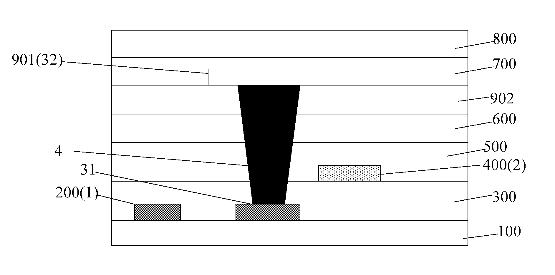
[0028]As described in BACKGROUND, the existing self-capacitive touch display device has a low accuracy of a touch operation. The inventor has found that, this issue is caused mainly by the fact that the distance between the conductive layer where line conductive portions are located and the conductive layer where touch electrodes are located is short, and the coupling capacitance between the touch line and the touch electrodes which the touch line passes by is large, thereby resulting in a low accuracy of a tou...


PUM


Abstract

An array substrate, a display panel, and a display device are disclosed. The array substrate includes: multiple gate lines, multiple data lines and multiple touch lines. The multiple data lines and multiple touch lines are insulated from each other, and extend in parallel directions. Each of the touch lines includes multiple line conductive portions and multiple connectors. The line conductive portions are located in the same layer with the gate lines and each of the line conductive portions is located between two adjacent gate lines. The connectors are located in a different conductive layer from the line conductive portions and the connectors connect two adjacent line conductive portions through a via hole. The coupling capacitance between the line conductive portions and the touch electrode positionally corresponding thereto may be reduced, to ensure a high accuracy of a touch operation for the display device.

Description

CROSS REFERENCE TO RELATED APPLICATIONS[0001]The present application claims the priority of Chinese Patent Application No. 201510153209.6, titled “ARRAY SUBSTRATE, DISPLAY PANEL AND DISPLAY DEVICE”, filed on Apr. 1, 2015 with the State Intellectual Property Office of People's Republic of China, which is incorporated herein by reference in its entirety.TECHNICAL FIELD[0002]The disclosure relates to the field of touch display technologies, and in particular to an array substrate, a display panel and a display device.BACKGROUND[0003]In the initial stages of development of touch display technologies, a touch display panel is formed by combining a touch panel and a display panel, to achieve a touch display function. The touch panel and the display panel are needed to be prepared separately, thereby resulting in high cost, a large thickness and low productivity.[0004]With the development of self-capacitive touch display integrated technology, a common electrode of the array substrate in t...

Claims


Application Information

Patent Timeline
Patent Type & Authority Applications(United States)
IPC IPC(8): G06F3/044
CPCG06F3/044G02F1/13338G06F3/0412G02F1/136286G06F3/0443G06F3/04164
Inventor DU, LINGXIAOYAO, QIJUN
Owner SHANGHAI TIANMA MICRO ELECTRONICS CO LTD
Why Eureka
Try Eureka