Array substrate, method for fabricating the same, and display apparatus

Active Publication Date: 2016-10-06
SHANGHAI TIANMA MICRO ELECTRONICS CO LTD +1
View PDF8 Cites 14 Cited by
  • Summary
  • Abstract
  • Description
  • Claims
  • Application Information

AI Technical Summary

Benefits of technology

[0019]With the array substrate fabricated using the fabricating method, light leakage at the gap between two adjacent electrode units due to the data lines can be avoided.
[0020]A display apparatus is further provided according to the present disclosure, which includes: the array substrate according to the present disclosure; and a cover plate

Problems solved by technology

However, the technology may result in light leakage of the liquid crystal displ

Method used


Image

  • Array substrate, method for fabricating the same, and display apparatus
  • Array substrate, method for fabricating the same, and display apparatus
  • Array substrate, method for fabricating the same, and display apparatus

Examples


Example

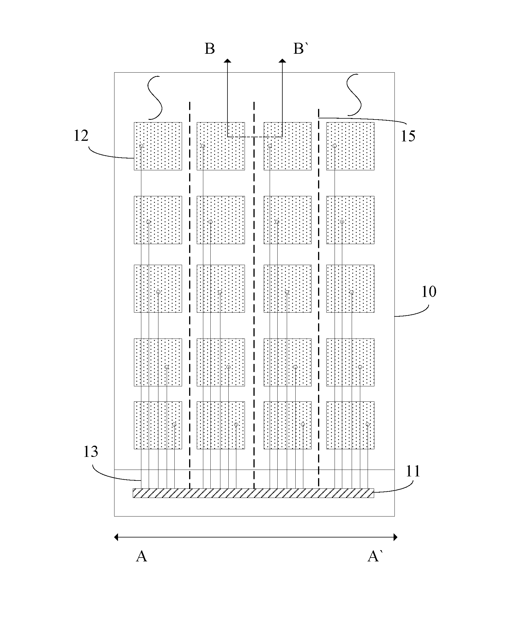
[0030]As described in the background, in the conventional in cell TP, a common electrode in a pixel area further serves as touch electrodes, and a volume of the in cell TP can be reduced. However, this technology may result in light leakage of the in cell TP. Specifically, reference is made to FIG. 1, which shows a schematic diagram of an in cell TP. A common electrode is disposed on an array substrate 10 of a liquid crystal display panel, for providing a common potential for pixel units (not shown in FIG. 1). In order to integrate touch function into the liquid crystal display panel, the common electrode is divided into multiple touch electrode units 12 independent from each other, and each of the touch electrode units 12 is connected, to a touch display chip 11 disposed on the array substrate 10, via a touch electrode lead 13. Operation time of the liquid crystal display panel includes a display phase and a touch sensing phase. In the display phase, the touch display chip 11 trans...


PUM


Abstract

An array substrate, a method for fabricating the same and a display apparatus are provided. The array substrate includes first non-display areas and second non-display areas, where the first non-display areas and the second non-display areas are respectively areas between adjacent columns of the pixel units and are arranged alternately in the first direction; two data lines are disposed in each first non-display area, the two data lines are electrically connected to two columns of pixel units on two sides of the first non-display area where the two data lines are located; a gap is provided between two electrode units adjacent in the first direction, and the gap is located above a part of the second non-display area.

Description

CROSS REFERENCE TO RELATED APPLICATIONS[0001]The present application claims the priority to Chinese Patent Application No. 201510152668.2, entitled “ARRAY SUBSTRATE, METHOD FOR FABRICATING THE SAME, AND DISPLAY APPARATUS”, filed on Apr. 1, 2015 with the State Intellectual Property Office of the Peoples Republic of China, which is incorporated herein by reference in its entirety.FIELD OF THE INVENTION[0002]The disclosure relates to the field of display technology, and in particular, to an array substrate, a method for fabricating the array substrate, and a display apparatus.BACKGROUND OF THE INVENTION[0003]As an input medium, a touch screen is an easy, convenient and natural device for human-computer interaction. Increasingly, it has become a research and development focus for flat panel display manufacturers to integrate a touch function into a liquid crystal display (LCD) or an organic light-emitting diode (OLED) display.[0004]In order to further reduce the volume of a touch screen...

Claims


Application Information

Patent Timeline
IPC IPC(8): G06F3/041
CPCG06F3/0416G06F2203/04111G06F2203/04103G02F1/13338G02F1/136227G02F1/136286G06F3/0412G06F3/04164G06F3/04184G06F3/0443G02F1/13629
Inventor LI, GUJUNSUN, YUNGANGYANG, KANG
Owner SHANGHAI TIANMA MICRO ELECTRONICS CO LTD
Why Eureka
Try Eureka