Image sensor and image capturing apparatus
a technology of image sensor and image sensor, which is applied in the direction of electrical equipment, radio frequency control devices, semiconductor devices, etc., can solve the problems of reducing and reducing the image quality. , to achieve the effect of suppressing the decrease of light and increasing the overall thickness of the image sensor
- Summary
- Abstract
- Description
- Claims
- Application Information
AI Technical Summary
Benefits of technology
Problems solved by technology
Method used
Image
Examples
first embodiment
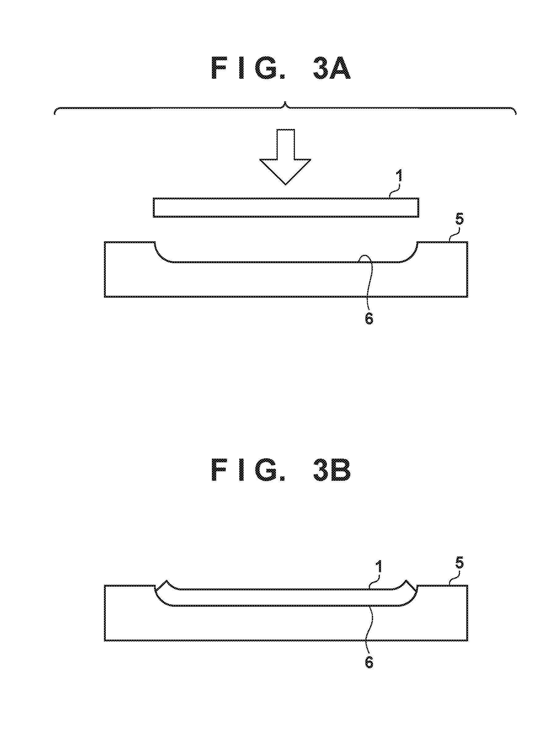
[0022]FIGS. 3A and 3B are diagrams showing a manufacturing method of an image sensor in a first embodiment. The image sensor of the present embodiment has an area that is flat (referred to below as a flat area) and an area that is curved (referred to below as a curved area) on the image sensing plane. As shown in FIG. 3A, the outer dimensions of a holding member 5 are greater than the image sensor 1, and a recessed portion 6 that includes a flat area and a curved area is formed in the upper surface of the holding member 5.
[0023]Stress is applied downward from the image sensing plane side of the image sensor 1 in a state where the image sensing plane is facing upward, so as to bring the image sensor 1 in contact with the recessed portion 6 of the holding member 5. This enables the shape of the image sensor 1 to be set to conform to the shape of the recessed portion 6, as shown in FIG. 3B. Also, the flat area and the curved area can be highly accurately formed in the image sensing pla...
second embodiment
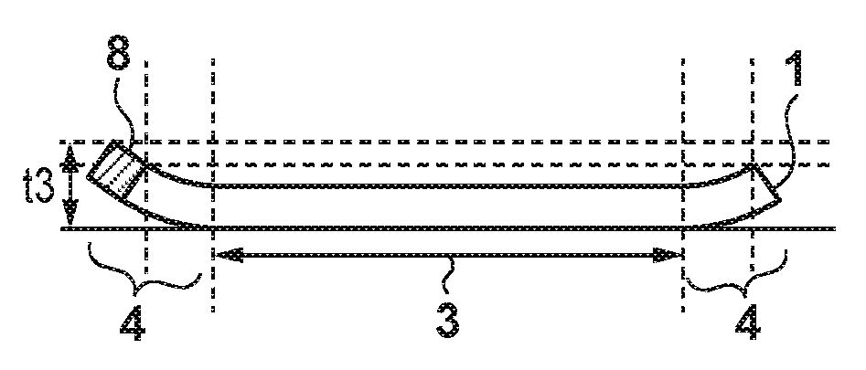
[0033]Hereinafter, an image sensor according to a second embodiment of the present invention will be described. FIG. 5 is a diagram showing the image sensing plane of the image sensor according to the second embodiment. The pixel area of the image sensor 1 in the present embodiment is provided with an effective pixel area 7 and a black reference pixel area 8 shown with a hatched pattern adjacent to the effective pixel area 7. The effective pixel area 7 is a pixel area having photoelectric conversion units that generate signal charges according to the received light amount. The black reference pixel area 8 is a shaded pixel area in which photoelectric conversion units are shaded with a wiring layer or the like. A black reference signal for determining a reference value (black level) for the output value of the effective pixel area 7 is output from this black reference pixel area 8. The black reference pixel area 8 is arranged on the upper side and the left side of the image sensor 1 ...
PUM
 Abstract
Description
Claims
Application Information


