led packaging method and led

A technology of LED packaging and LED chips, which is applied in the direction of electrical components, circuits, semiconductor devices, etc., can solve the problems of reduced luminous efficiency of phosphors, low excitation efficiency of phosphors, uneven distribution of phosphor layers, etc., so as to avoid the decline of luminous efficiency Effect

Inactive Publication Date: 2011-12-07
SHENZHEN JUFEI OPTOELECTRONICS
View PDF2 Cites 7 Cited by
  • Summary
  • Abstract
  • Description
  • Claims
  • Application Information

AI Technical Summary

Problems solved by technology

[0003] See figure 1 , the figure shows the existing LED packaging structure, including a bracket 1, the bracket 1 is provided with a cavity 2, the bottom of the cavity 2 is provided with a metal layer, an LED chip 4 is arranged on the metal layer, and the cavity 2 is filled with Fluorescent glue 3, after the filled fluorescent glue 3 is baked and formed, most of the fluorescent powder in the fluorescent glue 3 is deposited on the bottom of the cavity 2 and the surface of the LED chip 4, and the phosphor powder at the bottom of the cavity 2 is densely distributed , in the area away from the bottom of the cavity 2, there is only a little phosphor powder scattered, that is, the distribution of the phosphor layer formed after baking is very uneven
[0004] The above-mentioned LED packaging structure has the following problems: 1. Since the heat generated by the LED chip 4 is mainly transferred from the metal layer at the bottom of the cavity 2 to the outside of the cavity 2 in time, and figure 1 Most of the phosphor in the middle phosphor layer is deposited on the metal layer at the bottom of the cavity 2 and the surface of the LED chip 4, so the temperature on the LED chip 4 and the metal layer will first be transferred to the phosphor on the surface and close to the surface. , leading to an increase in the temperature of the phosphor, a decrease in the luminous efficiency of the phosphor, an increase in the attenuation speed of the phosphor, and an acceleration of the LED light decay
2. Due to figure 1 The phosphor powder in the middle phosphor powder layer is unevenly distributed, and the phosphor powder located on the surface of the metal layer and the LED chip 4 is deposited together, so that the phosphor powder accumulated together cannot be excited because it cannot absorb reflected light or scattered light, so its The excitation efficiency of the phosphor is low, and the uniformity of the light spot of the LED is poor

Method used


Image

  • led packaging method and led
  • led packaging method and led
  • led packaging method and led

Examples


Embodiment Construction

[0032] The present invention will be further described in detail below through specific embodiments in conjunction with the accompanying drawings.

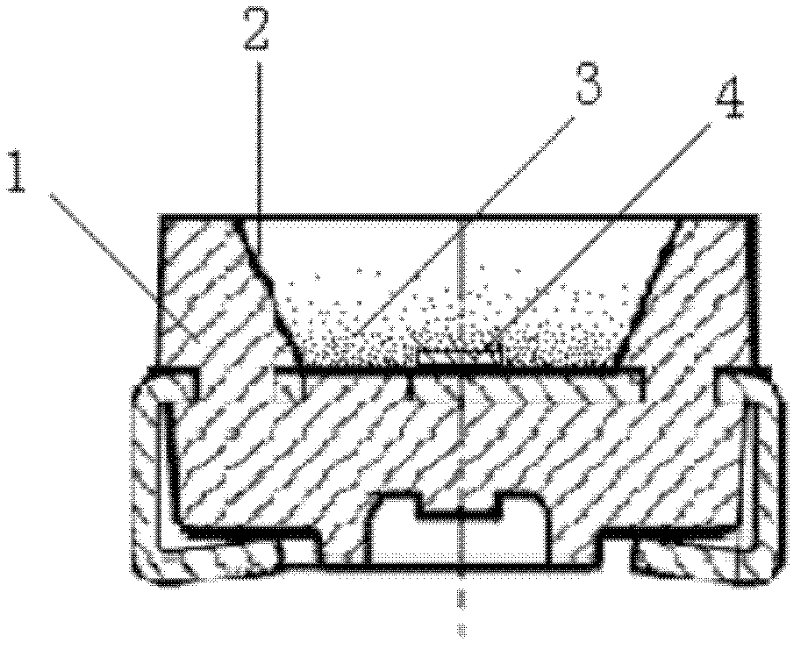
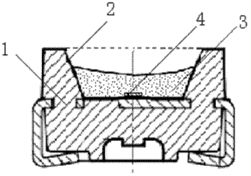
[0033] The LEDs in this example also include figure 1 As shown in the bracket 1 with a cavity 2 , the bottom of the cavity 2 is provided with a metal layer, and the LED chip 4 is arranged on the metal layer at the bottom of the cavity 2 . In order to better understand the present invention, the nouns used hereinafter are specifically explained below:

[0034] The colloid in this example refers to the colloid used for LED packaging, such as silica gel, silicone resin or epoxy resin;

[0035] The fluorescent glue in this example refers to the fluorescent glue that is prepared by mixing phosphor powder with glue in a certain proportion. The phosphor powder in the fluorescent glue is evenly distributed. It is worth noting that the fluorescent glue in this example can be a single phosphor or multiple A combination of phosphors.

[0...


PUM


Abstract

The invention discloses an LED packaging method and an LED, comprising filling a cavity with colloid, the filled colloid includes fluorescent glue, and then inverting the bracket filled with fluorescent glue so that the opening of the inverted bracket is downward, and the inverted The bracket is baked, so that the fluorescent glue in the cavity is cured and formed. During the baking molding process, due to the inversion of the bracket, the phosphor powder in the fluorescent glue will settle down due to gravity, so controlling the proper baking time and temperature can keep the final formed phosphor layer away from the metal layer at the bottom of the cavity And the LED chip arranged on the metal layer, avoiding the heat on the metal layer at the bottom of the cavity and the LED chip from being directly transferred to the phosphor powder in the phosphor powder layer, avoiding the decrease of luminous efficiency due to the rapid temperature rise of the phosphor powder in the phosphor powder layer, The phenomenon that the attenuation speed is accelerated and the LED light decay is accelerated.

Description

technical field [0001] The invention relates to the field of optoelectronic technology, in particular to an LED (light emitting diode) packaging method and the LED. Background technique [0002] At present, due to the advantages of high safety, stable operation, low energy consumption, high light efficiency, and long life, LEDs (light-emitting diodes) are more and more widely used in tablet computers, notebook computers, LCD monitors, large-size LCD TVs and Indoor lighting and outdoor lighting fields. As LEDs are more widely used and their quality requirements are higher, the light attenuation problem of LEDs has become a problem that people pay more and more attention to and urgently needs to be solved. [0003] See figure 1 , the figure shows the existing LED packaging structure, including a bracket 1, the bracket 1 is provided with a cavity 2, the bottom of the cavity 2 is provided with a metal layer, an LED chip 4 is arranged on the metal layer, and the cavity 2 is fil...

Claims


Application Information

Patent Timeline
Patent Type & Authority Applications(China)
IPC IPC(8): H01L33/00H01L33/48H01L33/50H01L33/64
Inventor 韦健华孙平如
Owner SHENZHEN JUFEI OPTOELECTRONICS
Why Eureka
Try Eureka