Touch panel and method of its manufacturing

a technology of touch panel and manufacturing method, which is applied in the field of touch panel, can solve the problems of not being able to easily not being able to exfoliate the various films of adhesive tape at a three-dimensionally formed portion having large undulation, and being difficult to realize the various combinations of conductive layers

Inactive Publication Date: 2016-10-20
HOSIDEN CORP
View PDF2 Cites 44 Cited by
  • Summary
  • Abstract
  • Description
  • Claims
  • Application Information

AI Technical Summary

Benefits of technology

[0018]In the above-described embodiment, after a multilayer film is shaped in the film shaping step, this formed multilayer film is placed in a mold and then an injection molding is effected, whereby a touch panel is manufactured. In the above, the multilayer film is produced in the film making step in which a conductive film having a conductive layer and a protective film are laminated to each other via an adhesive layer formed of a thermosetting type adhesive agent. At the time of completion of this film making step, the adhesive layer of the multilayer film has not yet been hardened, but the viscosity thereof keeps the conductive film and the protective film joined to each other. Then, when the temperature of the multilayer film rises above the setting (hardening or curing) temperature of the thermosetting resin by heating during or after the film shaping step subsequent thereto, the adhesive agent is hardened. As described, since hardening of the adhesive agent occurs n the film shaping step, distortion of the respective films which would otherwise occur during shaping can be suppressed. Consequently, it is possible to manufacture a touch panel in which a multilayer film having a stable three-dimensional shape and a panel member are integrated to each other. Further, even if the hardening of the adhesive layer fails to be completed by the heating in the film shaping step, this hardening of the adhesive agent can be completed appropriately later by reheating the multilayer film in the subsequent panel integrating step.

Problems solved by technology

However, with the arrangement of printing and laminating the decorative layer and the conductive layer on a single sheet of film, it is not readily possible to realize various combinations of the conductive layer and the decorative layer as desired.
However, since the adhesive bonding force of such adhesive tape is smaller than that of the adhesive bonding layer, exfoliation of the various films from the adhesive tape at a three-dimensionally formed portion having large undulation can occur.
For this reason, degree of freedom in the shape of films laminated on a touch panel would be limited.

Method used


Image

  • Touch panel and method of its manufacturing
  • Touch panel and method of its manufacturing
  • Touch panel and method of its manufacturing

Examples


first embodiment

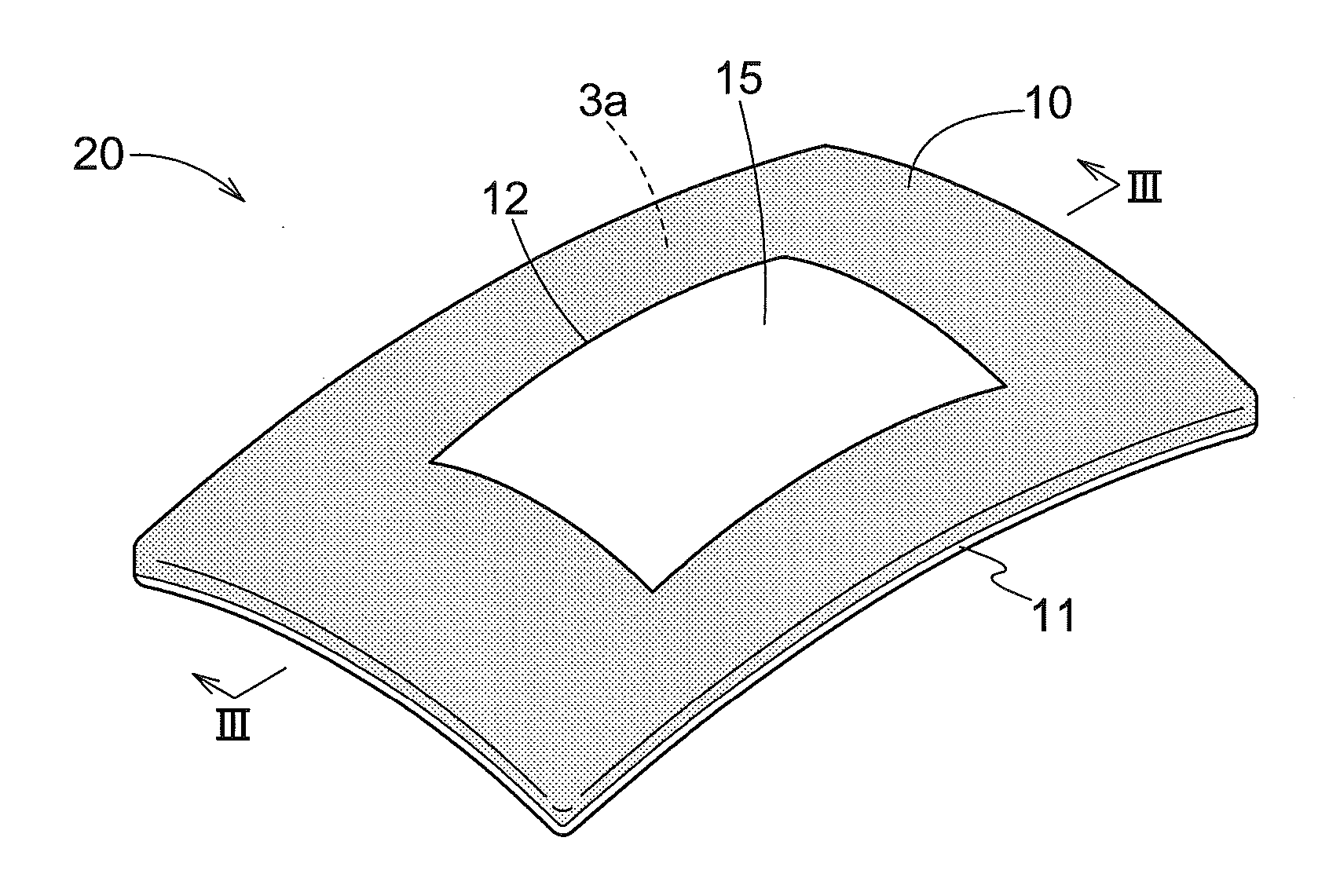
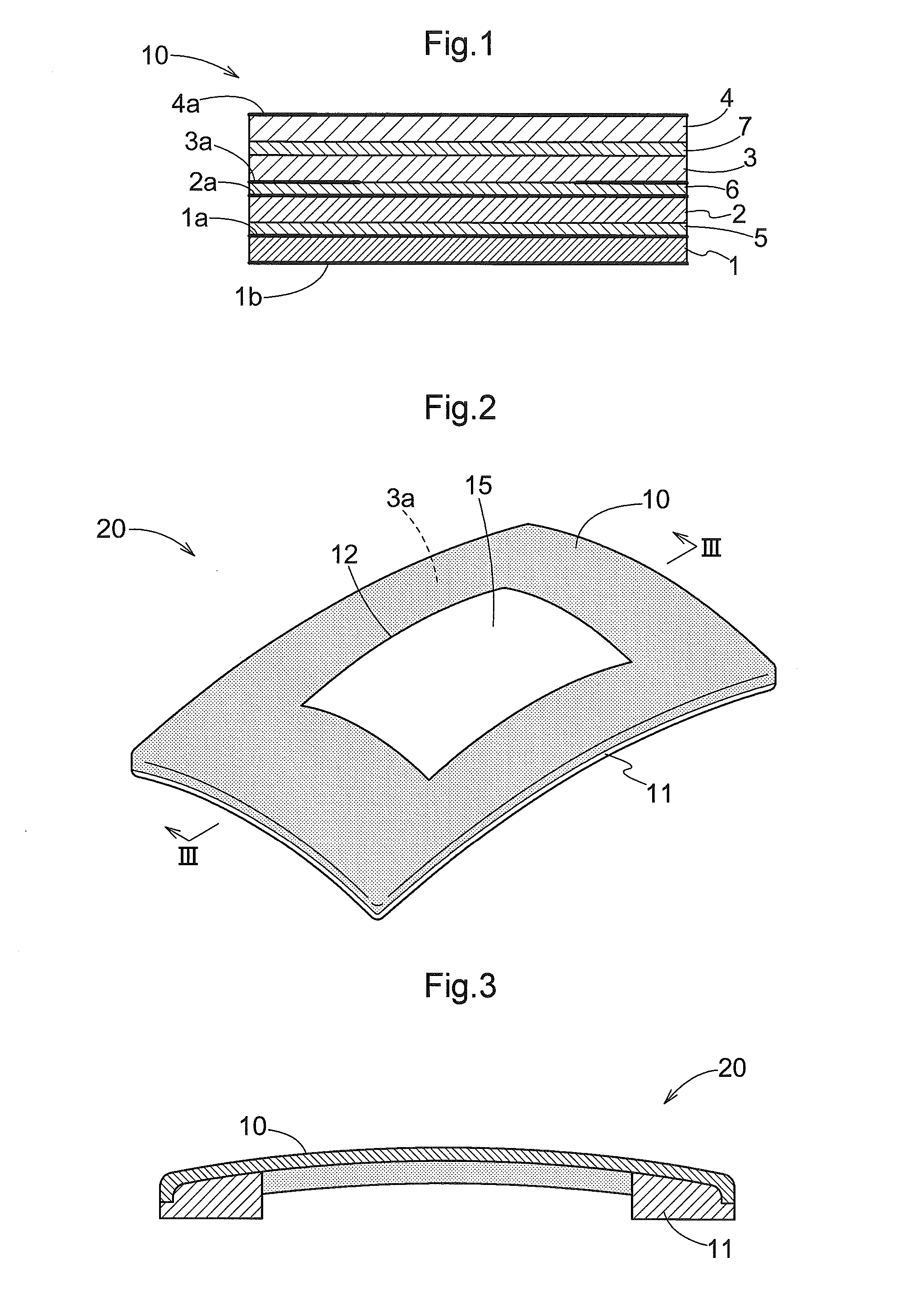
[0032]A touch panel 20, as shown in FIGS. 1-3, is formed by lamination of a multilayer film 10 on a front face of a panel member 11. The panel member 11 and the multilayer film 10 are both formed into a three-dimensional shape. In this embodiment, the front face of the touch panel 20 is formed into a three-dimensional curved shape. At a center of the panel, member 11, there is formed an aperture 12 which is form an operation screen of the touch panel 20.

[0033]As shown in FIG. 1, the multilayer film 10 includes first and second conductive films 1, 2 having first and second conductive layers 1a, 2a respectively, an adhesive layer 6, and a decorative film 3 having a decorative layer 3a, with these films and layers being laminated to each other one after another. On the front face side (the upper side in FIG. 1) of the decorative film 3, there is further laminated, via an adhesive layer 7, a protective film 4 having a protective layer 4a.

[0034]The first conductive film 1 and the second...

second embodiment

[0055]In a second embodiment, a touch panel 21, as shown in FIGS. 10-11, is configured such that the multilayer film 10 is laminated on the entire front face of a panel member 11 having no aperture. The panel member 11 and the multilayer film 10 are both formed into three-dimensional shape. The panel member 11 is formed of a transparent resin such as polycarbonate and formed into a shape approximately same as that of the multilayer film 10. In the multilayer film 10 shown in FIG. 10, no decorative layer 3a is formed in the light-transmitting region 15 which is to form the operation screen. Instead of this arrangement shown in FIG. 10, in the multilayer film 10, the decorative layer 3a can be formed at a part of the light-transmitting region 15. The touch panel 21 can be manufactured by the same manufacturing method as that employed in the first embodiment.

[0056]By forming the multilayer film 10 and the panel member 11 into a same shape and then laminating them to each other, it beco...


PUM

PropertyMeasurementUnit
temperatureaaaaaaaaaa

Abstract

A touch panel includes a panel member and a multilayer film joined to a front face of the panel member, the multilayer film including a conductive film having a conductive layer and a protective film. In the multilayer film, the respective films are laminated to each other via an adhesive layer formed of a thermosetting type adhesive agent and formed in a three-dimensional shape along the front face.

Description

CROSS REFERENCE TO RELATED APPLICATION[0001]This application is based on and claims priority under 35 U.S.C. Section 119 to Japanese Patent Application No. 2015-085887 filed on Apr. 20, 2015, and Japanese Patent Application No. 2016-039189 filed on Mar. 1, 2016, the entire content of each of which is incorporated herein by reference.TECHNICAL FIELD[0002]This disclosure relates to a touch panel and a method of its manufacturing.RELATED ART[0003]Conventionally, a touch panel has been used as an input device for an audio equipment of an automobile, a home electric appliance, an electronic device, etc. The touch panel is formed by printing and laminating a conductive layer for detecting an electrostatic capacity change and a decorative layer respectively on a front face of a film having insulating property. Use of the touch panel provides advantages such as possibility of forming an operating face flat, possibility of omitting various switching elements for input operations, and so on.[...

Claims


Application Information

Patent Timeline
Patent Type & Authority Applications(United States)
IPC IPC(8): G06F3/041B29C45/14
CPCG06F3/041G06F2203/04103B29C45/14G06F3/0414B32B7/12B32B15/08B32B15/082B32B15/085B32B15/09B32B23/00B32B23/042B32B27/26B32B27/281B32B27/308B32B27/32B32B27/325B32B27/36B32B27/365H03K17/962B32B2307/102B32B2307/202B32B2307/40B32B2307/412B32B2307/584B32B2307/71B32B2457/20B32B2457/202B32B2457/206B32B2457/208H03K2217/96031H03K2217/960755H03K2217/960785G06F1/1637G06F1/1643
Inventor ISODA, TAKESHIAO, HITOSHI
Owner HOSIDEN CORP
Why Eureka
Try Eureka