Amoled pixel driving circuit and pixel driving method

a driving circuit and pixel technology, applied in the field of display technology, can solve the problems of extremely affecting flowing through etc., and achieve the effect of improving the display effect of pictures and uniform brightness of the organic light emitting diodes

Active Publication Date: 2016-12-15
SHENZHEN CHINA STAR OPTOELECTRONICS TECH CO LTD
View PDF5 Cites 16 Cited by
  • Summary
  • Abstract
  • Description
  • Claims
  • Application Information

AI Technical Summary

Benefits of technology

[0007]An objective of the present invention is to provide an AMOLED pixel driving circuit, which can compensate the threshold voltage of the drive thin film transistor and stabili

Problems solved by technology

Thus, the current flowing through the organic light emitting diode is unstable and the brightness of the o

Method used


Image

  • Amoled pixel driving circuit and pixel driving method
  • Amoled pixel driving circuit and pixel driving method
  • Amoled pixel driving circuit and pixel driving method

Examples


Embodiment Construction

[0078]For better explaining the technical solution and the effect of the present invention, the present invention will be further described in detail with the accompanying drawings and the specific embodiments.

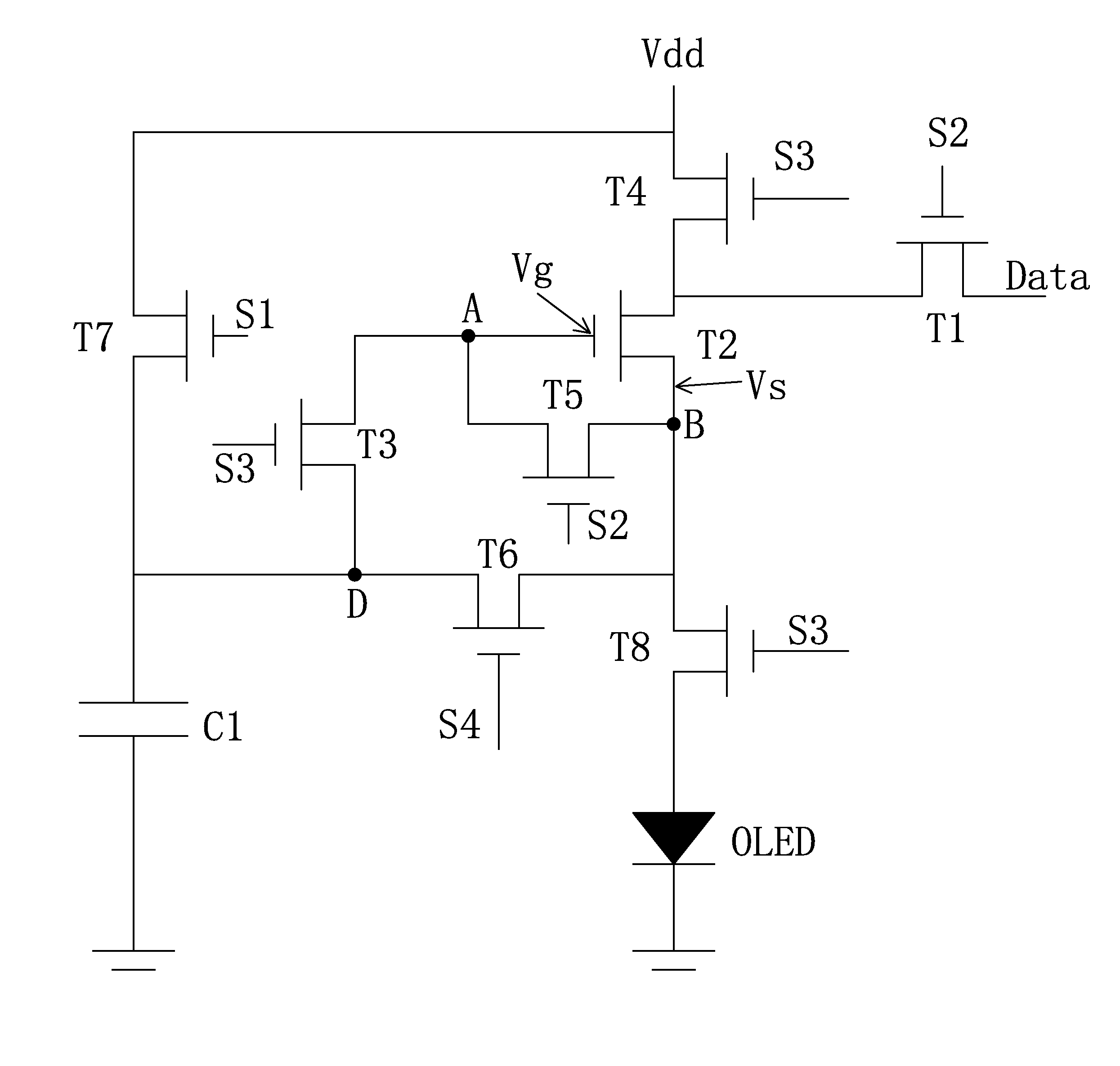
[0079]Please refer to FIG. 3, the present invention first provides an AMOLED pixel driving circuit. The AMOLED pixel driving circuit is a 8T1C structure, comprising: a first thin film transistor T1, a second thin film transistor T2, a third thin film transistor T3, a fourth thin film transistor T4, a fifth thin film transistor T5, a sixth thin film transistor T6, a seventh thin film transistor T7, an eighth thin film transistor T8, a capacitor C1 and an organic light emitting diode OLED.

[0080]A gate of the first thin film transistor T1 is electrically coupled to a second scan control signal S2, and a source is electrically coupled to a data signal Data, and a drain is electrically coupled to a source of the fourth thin film transistor T4 and a drain of the second thin film tra...


PUM


Abstract

The present invention provides an AMOLED pixel driving circuit and a pixel driving method. The AMOLED pixel driving circuit utilizes a 8T1C structure, comprising a first, a second, a third, a fourth, a fifth and a sixth, a seventh and an eighth thin film transistors (T1, T2, T3, T4, T5, T6, T7, T8), a capacitor (C1) and an organic light emitting diode (OLED). The AMOLED pixel driving circuit, by directly gaining the second thin film transistor (T2), i.e. the drive thin film transistor, can effectively compensate the threshold voltage of the drive thin film transistor and stabilize the current flowing through the organic light emitting diode (OLED) to ensure the uniform brightness of the organic light emitting diode (OLED) and improve the display effect of the pictures. The unnecessary irradiance of the organic light emitting diode (OLED) can be avoided to reduce the electrical power consumption.

Description

FIELD OF THE INVENTION[0001]The present invention relates to a display technology field, and more particularly to an AMOLED pixel driving circuit and a pixel driving method.BACKGROUND OF THE INVENTION[0002]The Organic Light Emitting Display (OLED) possesses many outstanding properties of self-illumination, low driving voltage, high luminescence efficiency, short response time, high clarity and contrast, near 180° view angle, wide range of working temperature, applicability of flexible display and large scale full color display. The OLED is considered as the most potential display device.[0003]The OLED can be categorized into two major types according to the driving methods, which are the Passive Matrix OLED (PMOLED) and the Active Matrix OLED (AMOLED), i.e. two types of the direct addressing and the Thin Film Transistor (TFT) matrix addressing. The AMOLED comprises pixels arranged in array and belongs to active display type, which has high lighting efficiency and is generally utiliz...

Claims


Application Information

Patent Timeline
IPC IPC(8): G09G3/3258G09G3/3233
CPCG09G3/3258G09G2300/0819G09G2320/0233G09G2300/0842G09G2320/045G09G3/3233G09G2300/0861G09G2310/0262G09G2320/043
Inventor WU, XIAOLING
Owner SHENZHEN CHINA STAR OPTOELECTRONICS TECH CO LTD
Why Eureka
Try Eureka