Organic light emitting display device

a light-emitting display and organic technology, applied in semiconductor devices, instruments, electrical devices, etc., to achieve the effect of stably receiving data signals, reducing or preventing coupling, and reducing or preventing interference of data signals

Active Publication Date: 2017-01-26
SAMSUNG DISPLAY CO LTD
View PDF7 Cites 16 Cited by
  • Summary
  • Abstract
  • Description
  • Claims
  • Application Information

AI Technical Summary

Benefits of technology

[0007]Embodiments of the present invention relate to organic light emitting display devices capable of reducing or preventing coupling (such as capacitive coupling) from being generated between adjacent data lines and reducing or preventing interference of data signals so that pixels emit light with desired brightness.
[0021]In organic light emitting display devices according to embodiments of the present invention, it is possible to reduce or prevent coupling (e.g., capacitive coupling) from being generated between adjacent data lines so that it is possible to reduce or prevent interference of data signals. Therefore, pixels may stably receive the data signals and may emit light with desired brightness.

Problems solved by technology

However, when data lines that supply data signals to different pixels are adjacent to each other (such as side-by-side or without any circuits between them), coupling (such as capacitive coupling) may be generated between the data lines so that the pixels of the organic light emitting display device may not emit light with desired brightness.

Method used


Image

  • Organic light emitting display device
  • Organic light emitting display device
  • Organic light emitting display device

Examples


Embodiment Construction

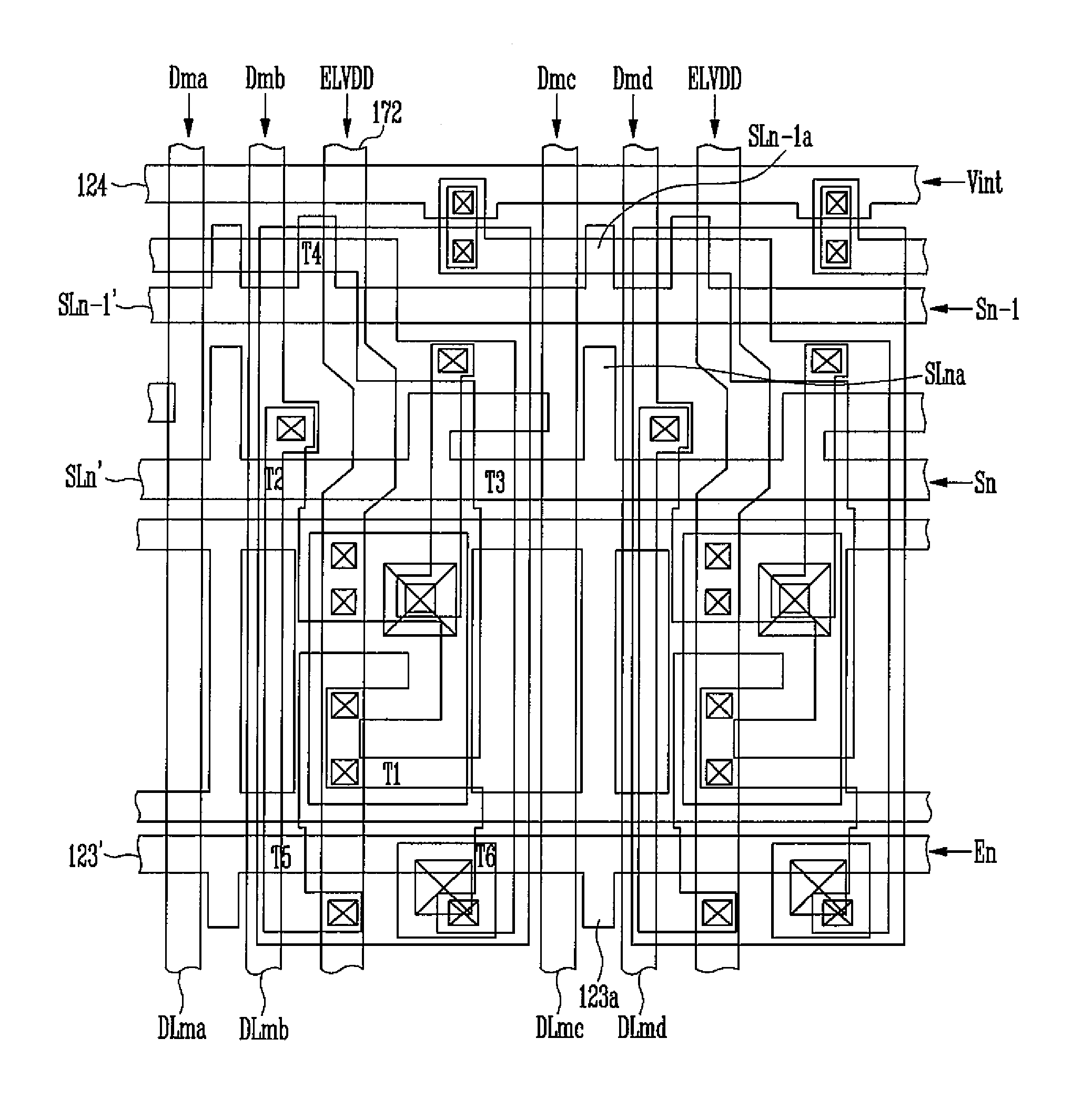
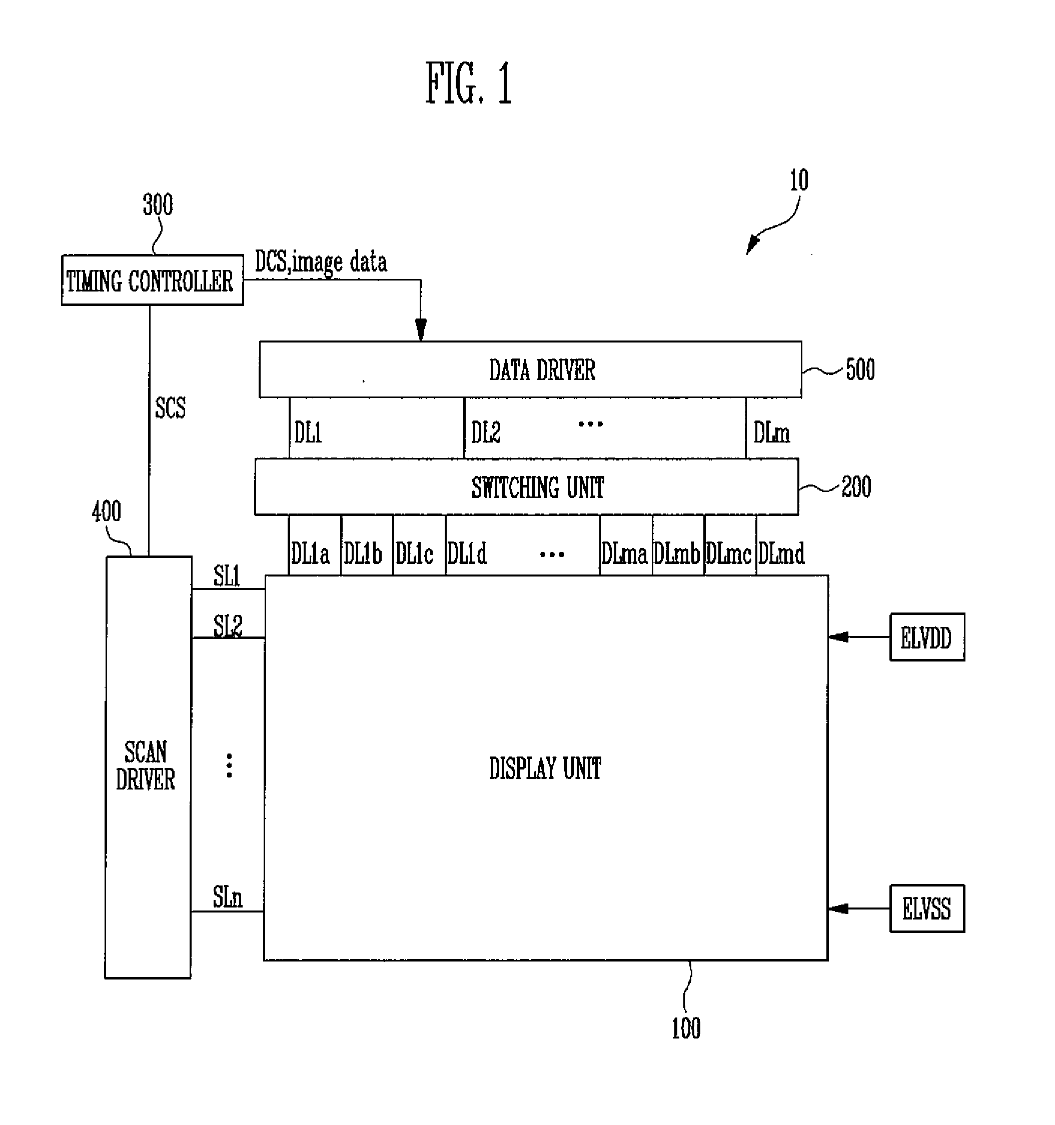
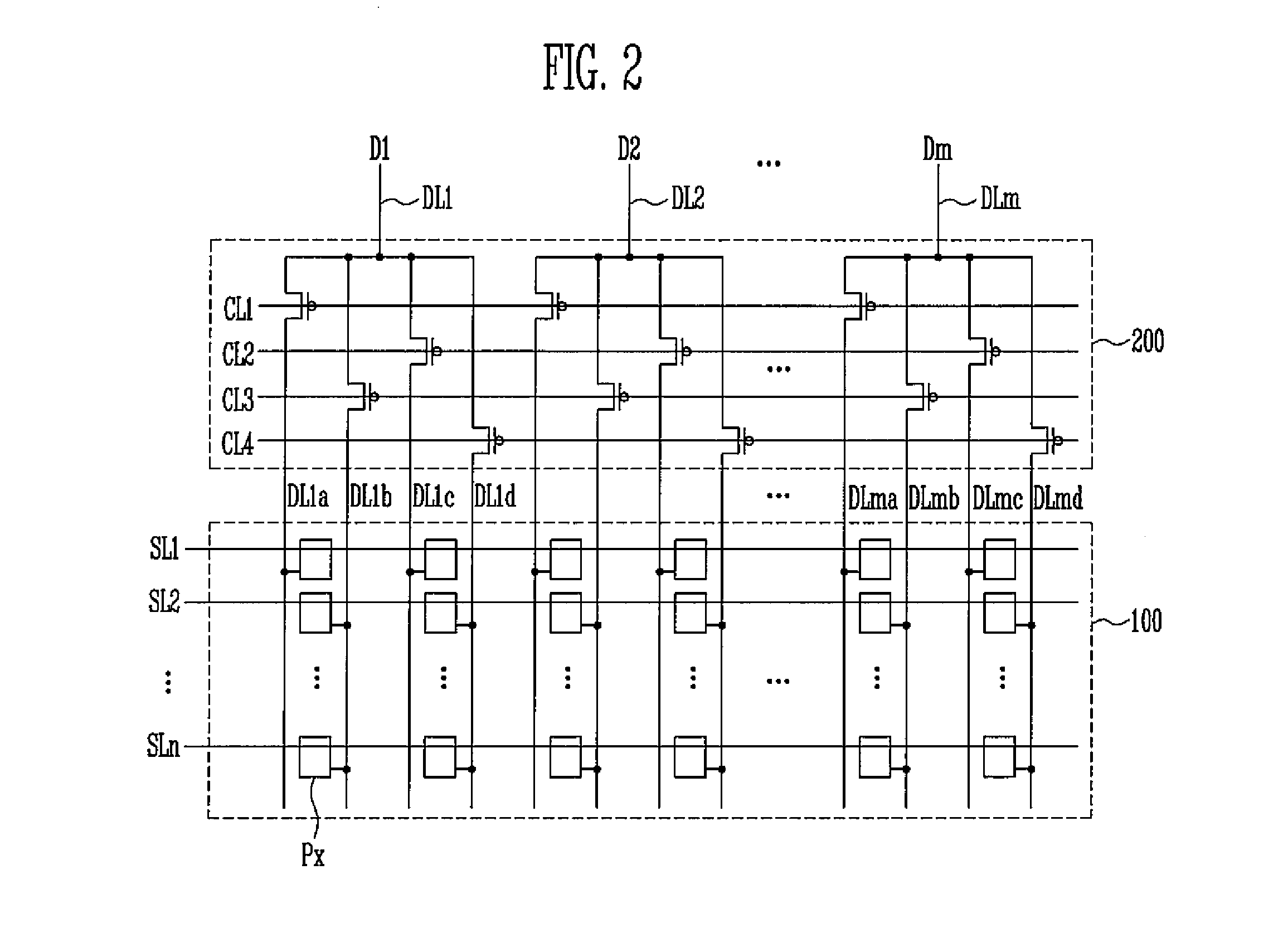
[0030]Embodiments of the present invention will now be described more fully with reference to the accompanying drawings. The present invention may, however, be embodied in many different forms and should not be construed as limited to the embodiments set forth herein. Rather, these embodiments are provided to more fully convey the scope of the present invention to one of ordinary skill in the art.

[0031]In the drawing figures, dimensions may be exaggerated for clarity of illustration. It will be understood that when an element is referred to as being “between” two elements, it can be the only element between the two elements, or one or more intervening elements may also be present. Like or similar reference numerals refer to like or similar elements throughout.

[0032]It will be understood that, although the terms first and second, etc., may be used herein to describe various elements, these elements should not be limited by these terms. These terms are mainly used to distinguish one e...


PUM


Abstract

An organic light emitting display device includes a substrate on which is included pixel columns extending in a column direction and adjacent to each other in a row direction, data lines extending in the column direction and adjacent to each other and between the pixel columns in the row direction, a power source line extending in the column direction, a scan line extending in the row direction, a switching transistor connected to the scan line and one of the data lines, a driving transistor connected to the switching transistor, an OLED connected to the driving transistor, and a storage capacitor including a first storage capacitor plate and a second storage capacitor plate overlapping the first storage capacitor plate in a thickness direction, connected to the power source line, and having a portion extending in the column direction between and not overlapping the data lines in the thickness direction.

Description

CROSS-REFERENCE TO RELATED APPLICATION[0001]This application claims priority to and the benefit of Korean Patent Application No. 10-2015-0104560, filed on Jul. 23, 2015 in the Korean Intellectual Property Office, the entire content of which is incorporated herein by reference.BACKGROUND[0002]1. Field[0003]Aspects of embodiments of the present invention relate to an organic light emitting display device.[0004]2. Description of the Related Art[0005]Recently, various display devices having reduced weight and volume compared to those of cathode ray tube devices have been developed. These display devices include, for example, liquid crystal display devices, field emission display devices, plasma display panels, and organic light emitting display devices.[0006]Organic light emitting display devices include pixels that display images and apply currents to organic light emitting diodes (OLEDs) included in the pixels to display the images. The pixels emit light corresponding to data signals ...

Claims


Application Information

Patent Timeline
Patent Type & Authority Applications(United States)
IPC IPC(8): H01L27/32
CPCH01L27/3248H01L27/3265H01L27/3262H01L27/3276G09G3/32H10K59/1216H10K59/131H10K59/123H10K59/124H10K59/1213
Inventor BYUN, MIN WOOPARK, KYOUNG JIN
Owner SAMSUNG DISPLAY CO LTD
Why Eureka
Try Eureka