Multi-terminal chip inductor

Pending Publication Date: 2022-02-24
MURATA MFG CO LTD
View PDF0 Cites 0 Cited by
  • Summary
  • Abstract
  • Description
  • Claims
  • Application Information

AI Technical Summary

Benefits of technology

[0009]With the above configuration, a plurality of coil conductors connected in parallel are used regardless of the inductance value to be selected. This effectively increases the Q factor of the inductance element observed from each external electrode.
[001

Problems solved by technology

However, when the plurality of independent coils are provided in this manner, the coils interfere with each other, a

Method used


Image

  • Multi-terminal chip inductor
  • Multi-terminal chip inductor
  • Multi-terminal chip inductor

Examples


first preferred embodiment

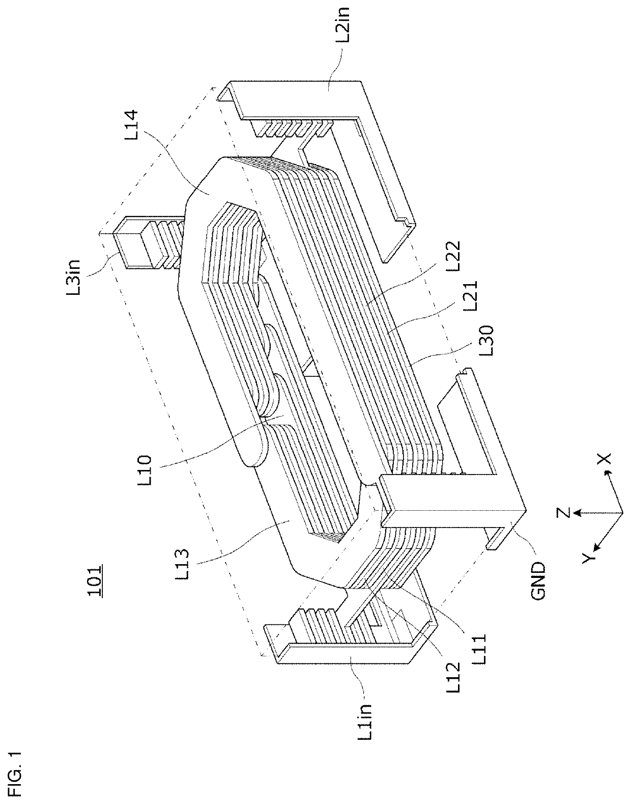
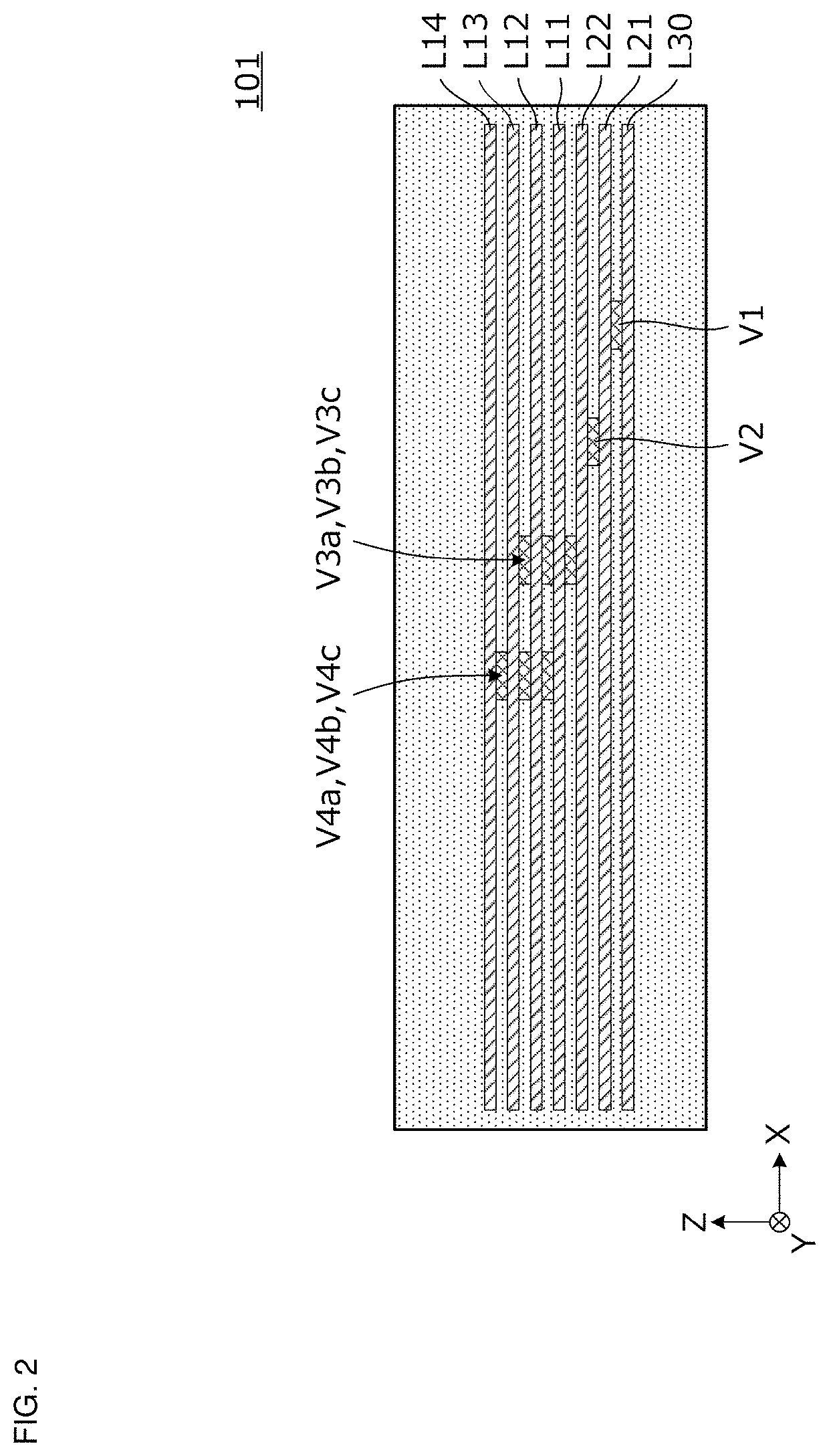
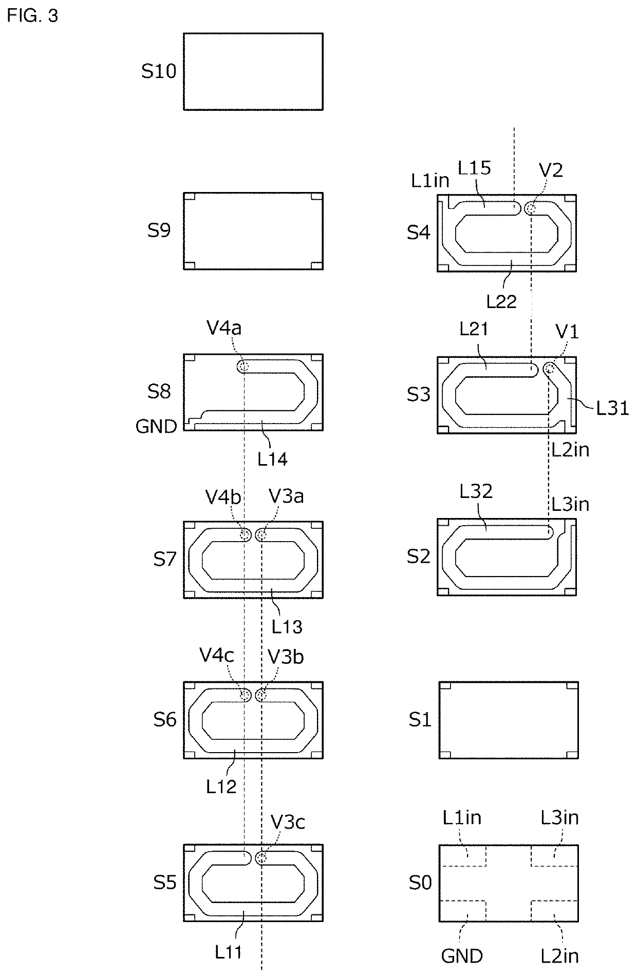
[0021]FIG. 1 is a transparent perspective view of a multi-terminal chip inductor 101 according to a first preferred embodiment of the present invention illustrating an internal structure. FIG. 2 is a front view of the multi-terminal chip inductor 101 in FIG. 1 viewed in a Y direction of an XYZ coordinate system. Note that external electrodes, which will be described later, are not illustrated. FIG. 3 is an exploded plan view of the multi-terminal chip inductor 101 illustrating a conductor pattern formed in each base material layer. FIG. 4 is a circuit diagram of the multi-terminal chip inductor 101.

[0022]The multi-terminal chip inductor 101 includes a plurality of base material layers S1 to S10, a plurality of coil conductors each provided in a predetermined plurality of base material layers S2 to S8 among the plurality of base material layers S1 to S10, an interlayer connection conductor connecting the plurality of coil conductors across layers, and a plurality of external electrod...

second preferred embodiment

[0053]In a second preferred embodiment of the present invention, a multi-terminal chip inductor including a smaller number of external electrodes than the multi-terminal chip inductor described in the first preferred embodiment is exemplified.

[0054]FIG. 6 is a circuit diagram of a multi-terminal chip inductor 102 according to the second preferred embodiment. In the multi-terminal chip inductor 102, the first coil conductor L10, which is connected between the common external electrode GND and the external electrode L1in adjacent to the external electrode GND in the circuit, includes a parallel connection circuit of the first coil conductors L11 and L12.

[0055]As illustrated in the second preferred embodiment, the present invention may also be applied to a multi-terminal chip inductor including only the three external electrodes L1in, L2in, and GND as external electrodes.

[0056]Finally, the above description of the preferred embodiments is illustrative in all respects and not restrictiv...


PUM


Abstract

A multi-terminal chip inductor includes coil conductors in base material layers, an interlayer connection conductor connecting the coil conductors across layers, and external electrodes each connected to portions of a series of coil conductors defined by the coil conductors and the interlayer connection conductor. The external electrodes include a common external electrode. A first of the coil conductors to which the common external electrode and a first external electrode adjacent to the common external electrode in a circuit are connected, includes first coil conductors connected to each other in parallel.

Description

CROSS REFERENCE TO RELATED APPLICATIONS[0001]This application claims the benefit of priority to Japanese Patent Application No. 2019-233777 filed on Dec. 25, 2019 and is a Continuation Application of PCT Application No. PCT / JP2020 / 043986 filed on Nov. 26, 2020. The entire contents of each application are hereby incorporated herein by reference.BACKGROUND OF THE INVENTION1. Field of the Invention[0002]The present invention relates to a multi-terminal chip inductor including a coil conductor in a multilayer body including a plurality of base material layers and used as an element including a plurality of inductance values.2. Description of the Related Art[0003]In the past, a laminated inductance element having a plurality of inductance values has been formed by providing a coil conductor in a multilayer body of base material layers.[0004]For example, Japanese Unexamined Patent Application Publication No. 10-208943 discloses a laminated inductance element in which a spiral laminated co...

Claims


Application Information

Patent Timeline
IPC IPC(8): H01F27/28H01F27/29
CPCH01F27/2804H01F2027/2809H01F27/29H01F17/0013H01F27/292H01F2021/125
Inventor SHIGEMATSU, SATOSHIISHIZUKA, KENICHI
Owner MURATA MFG CO LTD
Why Eureka
Try Eureka