Thin film deposition apparatus

a thin film deposition and film technology, applied in the direction of chemically reactive gases, coatings, crystal growth processes, etc., can solve the problems of process equipment lifespan decline, process negatively affected, outer chamber components,

Active Publication Date: 2017-02-16
ASM IP HLDG BV
View PDF3 Cites 203 Cited by
  • Summary
  • Abstract
  • Description
  • Claims
  • Application Information

AI Technical Summary

Benefits of technology

[0010]According to one or more embodiments, the above-mentioned problems (such as the deformation of an outer cham

Problems solved by technology

However, gas leakage that occurs when multiple reactor apparatuses are used leads to various problems during processes performed in the multiple reactor apparatuses.
For example, the supply of sources and reaction gases to substrates may be disturbed, and thus, processes may be negatively affected.
In addition, corrosion of outer chamber compon

Method used


Image

  • Thin film deposition apparatus
  • Thin film deposition apparatus
  • Thin film deposition apparatus

Examples


Embodiment Construction

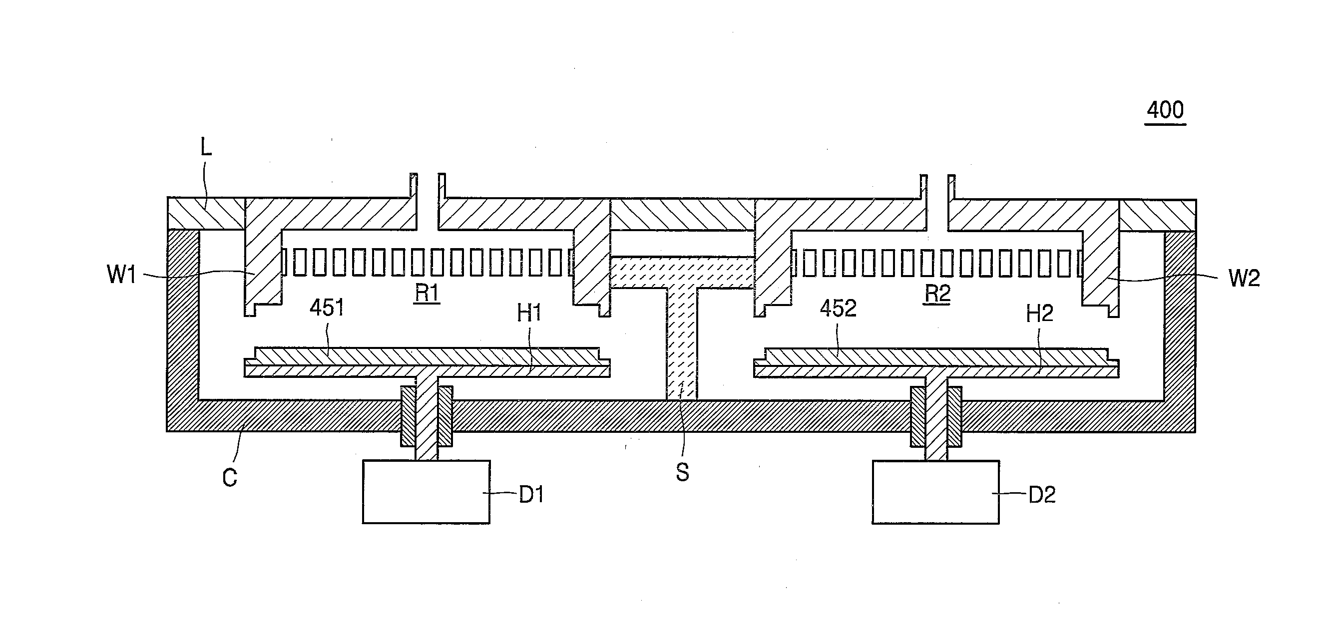
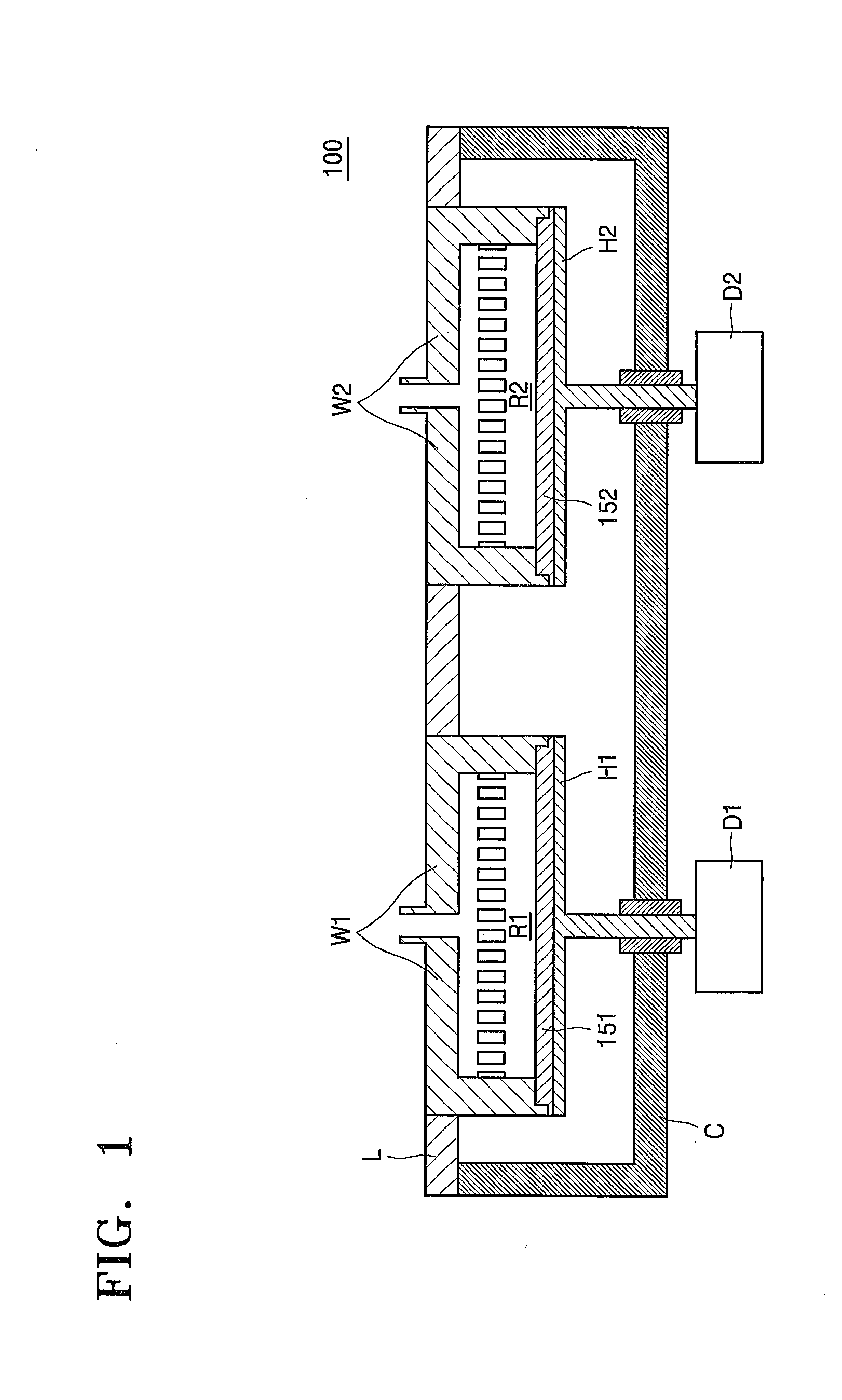
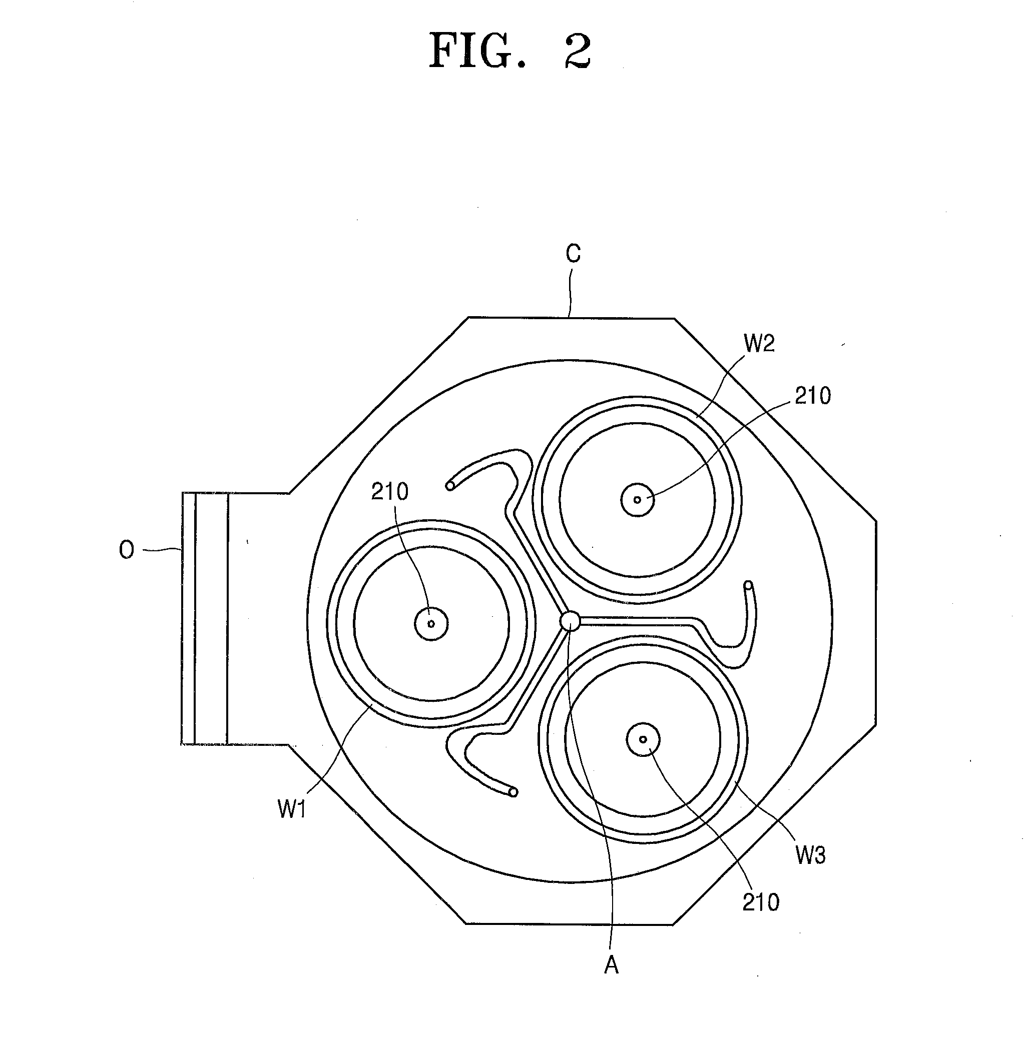
[0045]Reference will now be made in detail to embodiments, examples of which are illustrated in the accompanying drawings, wherein like reference numerals refer to like elements throughout. In this regard, the present embodiments may have different forms and should not be construed as being limited to the descriptions set forth herein. Accordingly, the embodiments are merely described below, by referring to the figures, to explain aspects of the present description. As used herein, the term “and / or” includes any and all combinations of one or more of the associated listed items. Expressions such as “at least one of,” when preceding a list of elements, modify the entire list of elements and do not modify the individual elements of the list.

[0046]Embodiments will now be described with reference to the accompanying drawings.

[0047]The inventive concept may, however, be embodied in many different forms and should not be construed as being limited to the embodiments set forth herein; rath...


PUM

PropertyMeasurementUnit
Pressureaaaaaaaaaa
Shapeaaaaaaaaaa
Widthaaaaaaaaaa

Abstract

Disclosed are a substrate holder and a semiconductor manufacturing apparatus including the substrate holder. The substrate holder provides a reaction region by making face-sealing contact with a reactor wall. The substrate holder has an elastic behavior when pressure is applied thereto while the substrate holder makes face-sealing contact with the reactor wall. The semiconductor manufacturing apparatus includes the substrate holder and a gas supply unit configured to supply gas to the reaction region provided by the reactor wall and the substrate holder.

Description

CROSS-REFERENCE TO RELATED APPLICATION[0001]This application claims the benefit of Korean Patent Application No. 10-2015-0114564, filed on Aug. 13, 2015 in the Korean Intellectual Property Office, and No. 10-2016-0073841, filed on Jun. 14, 2016 in the Korean Intellectual Property Office, the disclosure of which is incorporated herein in its entirety by reference.BACKGROUND[0002]1. Field[0003]One or more embodiments relate to a substrate holder and a semiconductor manufacturing apparatus (such as a thin film deposition apparatus) including the substrate holder.[0004]2. Description of the Related Art[0005]Recently, the line width of semiconductor circuits has been decreased to twenty or twenty-plus nanometers (nm), and thus, it is necessary to deposit very thin films on silicon substrates and tighten the conditions for thin film deposition processes. In addition, it is necessary to increase the throughput of systems or processes to realize commercial mass production.[0006]Deposition r...

Claims


Application Information

Patent Timeline
IPC IPC(8): C23C16/458C23C16/455
CPCC23C16/4585C23C16/45565C23C16/4586C23C16/4409C23C16/4581C30B25/12
Inventor JANG, HYUN SOOKEE, JEONG HOKIM, WOO CHANJUN, SUNG HOONSHON, JONG WON
Owner ASM IP HLDG BV
Why Eureka
Try Eureka