

Capacitive force sensing touch panel
- Summary
- Abstract
- Description
- Claims
- Application Information
AI Technical Summary
Benefits of technology
Problems solved by technology
Method used
Image

Examples
Embodiment Construction
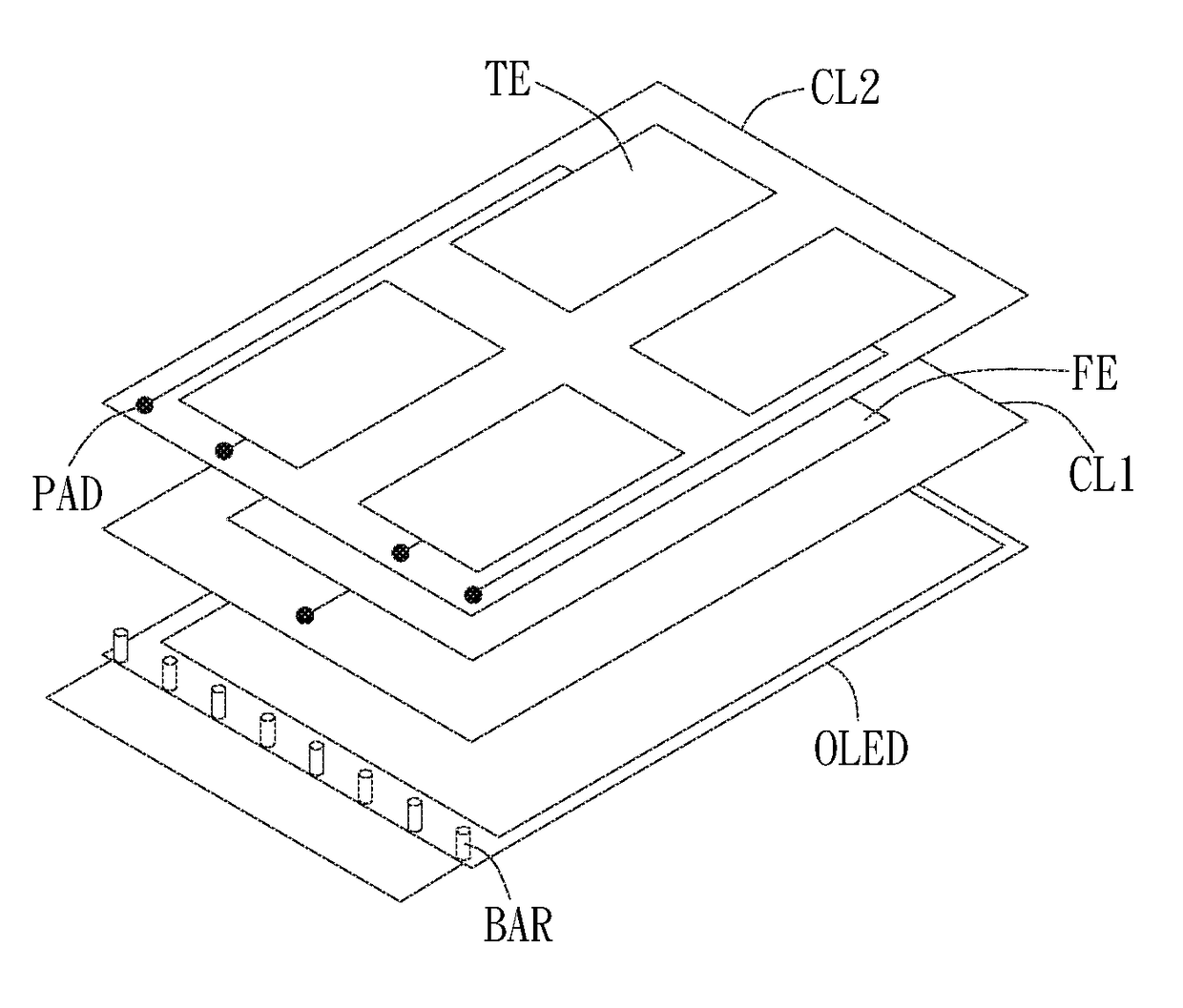
[0066]A preferred embodiment of the invention is a capacitive force sensing touch panel. In this embodiment, the capacitive force sensing touch panel can have different touch panel structures such as in-cell touch panel structure, on-cell touch panel structure or out-cell touch panel structure, and the capacitive force sensing touch panel can be an OLED display panel, but not limited to this.
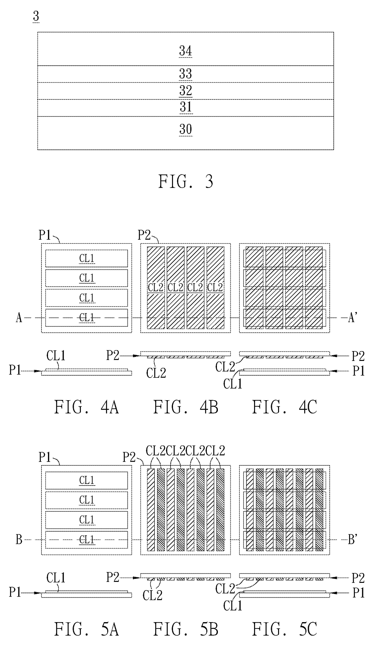
[0067]Please refer to FIG. 3. FIG. 3 illustrates a schematic diagram of the laminated structure of the pixel of the OLED display panel. AS shown in FIG. 3, the laminated structure 3 includes a first substrate 30, an anode layer 31, an OLED layer 32, a cathode layer 33 and a second substrate 34. Wherein, the anode layer 31 is disposed between the first substrate 30 and the OLED layer 32; the cathode layer 33 is disposed between the OLED layer 32 and the second substrate 34.
[0068]It should be noticed that, in the laminated structure of the pixel of the capacitive force sensing touch panel of the i...
PUM
 Abstract
Description
Claims
Application Information