
Chip package and method for forming the same

a chip and package technology, applied in the direction of semiconductor devices, semiconductor/solid-state device details, electrical apparatus, etc., can solve the problems of difficult to further reduce the size of an electronic product formed using the chip package, the attenuation of the power and/or signal of the electronic product is great, and the circuit board size is limited

Inactive Publication Date: 2017-04-27
XINTEC INC
View PDF0 Cites 1 Cited by
  • Summary
  • Abstract
  • Description
  • Claims
  • Application Information

AI Technical Summary

Benefits of technology

The patent text explains a problem where circuit boards are limited in size, making it difficult to make smaller electronic products. Additionally, long electrical transfer paths between the chip package and other electronic elements lead to reduced power and signal quality, increased noise, and lower overall quality of the electronic product. This technical effect limits the performance of electronic products.

Problems solved by technology

However, the size of the circuit board is limited.
As a result, it is difficult to further decrease the size of an electronic product formed using the chip package.
Furthermore, since electrical transfer paths between the chip package and another electronic element are long, attenuation of the power and / or signal of the electronic product is great.
Also, noise is easily induced.
Therefore, the quality of the electronic product is reduced.

Method used


Image

  • Chip package and method for forming the same
  • Chip package and method for forming the same
  • Chip package and method for forming the same

Examples


Embodiment Construction

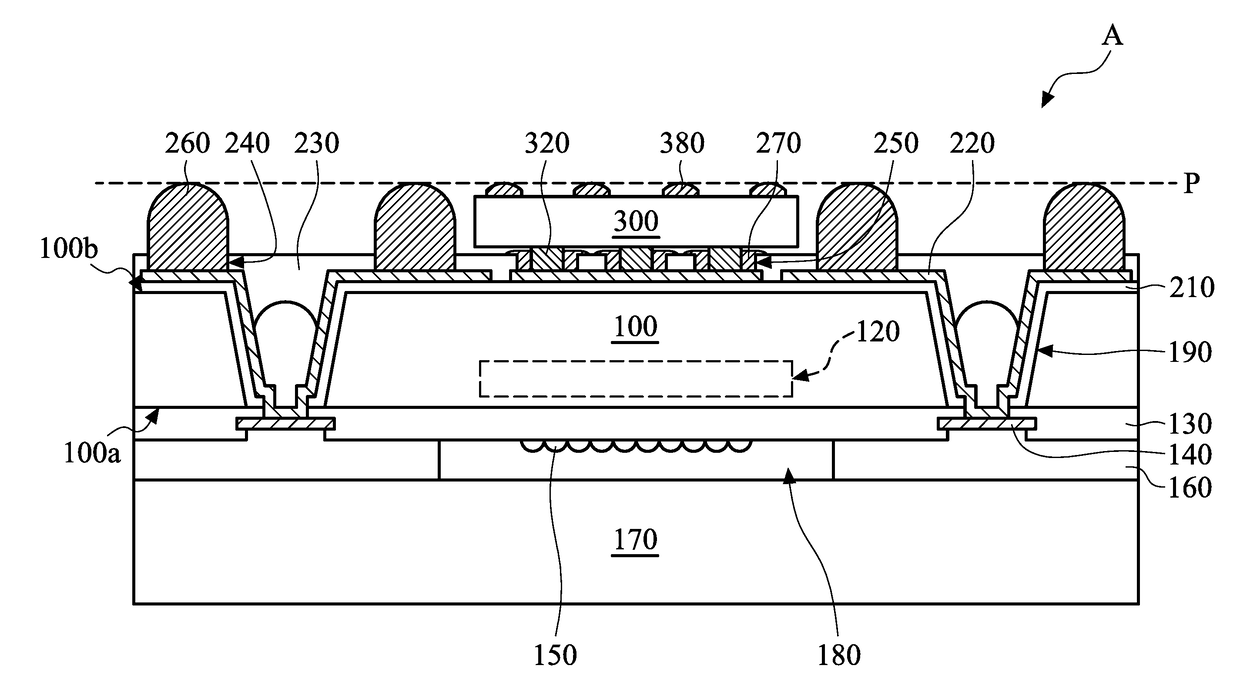
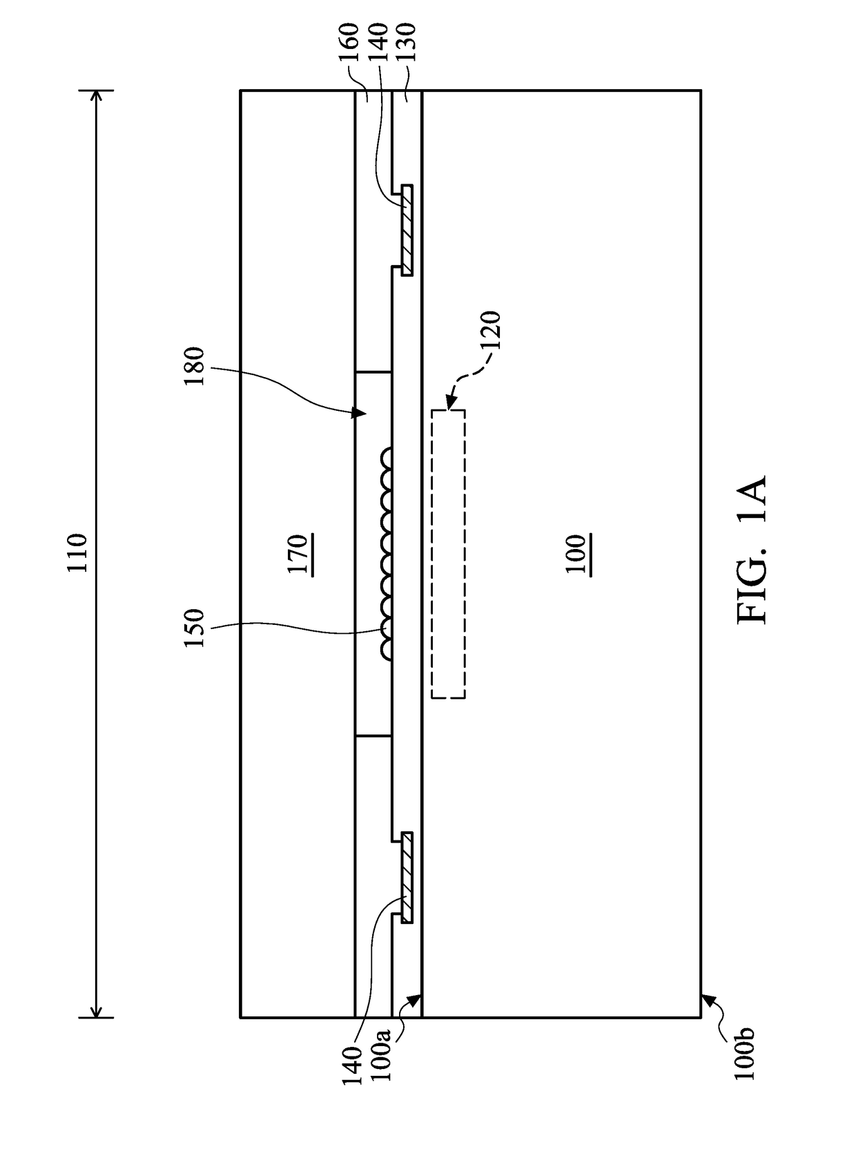
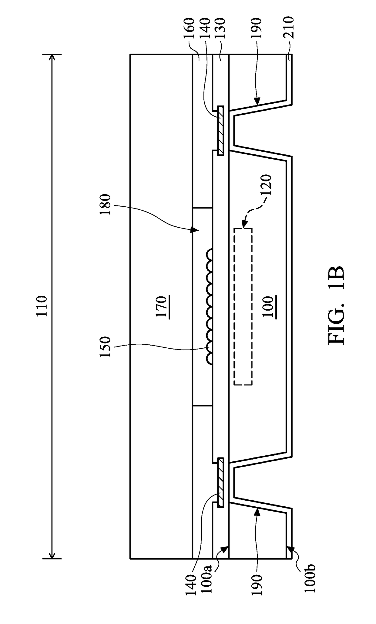
[0014]The making and using of the embodiments of the present disclosure are discussed in detail below. However, it should be noted that the embodiments provide many applicable inventive concepts that can be embodied in a variety of specific methods. The specific embodiments discussed are merely illustrative of specific methods to make and use the embodiments, and do not limit the scope of the disclosure. The disclosed contents of the present disclosure include all the embodiments derived from claims of the present disclosure by those skilled in the art. In addition, the present disclosure may repeat reference numbers and / or letters in the various embodiments. This repetition is for the purpose of simplicity and clarity, and does not imply any relationship between the different embodiments and / or configurations discussed. Furthermore, when a first layer is referred to as being on or overlying a second layer, the first layer may be in direct contact with the second layer, or spaced ap...


PUM


Abstract

A chip package is provided. The chip package includes a substrate. The substrate includes a sensing region or device region. The chip package also includes a first conducting structure disposed on the substrate. The first conducting structure is electrically connected to the sensing region or device region. The chip package further includes a passive element vertically stacked on the substrate. The passive element and the first conducting structure are positioned side by side.

Description

CROSS REFERENCE TO RELATED APPLICATIONS[0001]This Application claims priority of U.S. Provisional Application No. 62 / 244,593, filed Oct. 21, 2015, the entirety of which is incorporated by reference herein.BACKGROUND OF THE INVENTION[0002]Field of the Invention[0003]The invention relates to chip package technology, and in particular to a chip package having a passive element and methods for forming the same.[0004]Description of the Related Art[0005]The chip packaging process is an important step in the fabrication of an electronic product. Chip packages not only protect the chips therein from outer environmental contaminants, but they also provide electrical connection paths between electronic elements inside and those outside of the chip packages.[0006]In general, a chip package and another electronic element (such as a passive element) are disposed on a circuit board independently, and are indirectly electrically connected to each other. However, the size of the circuit board is li...

Claims


Application Information

Patent Timeline
Patent Type & Authority Applications(United States)
IPC IPC(8): H01L23/00
CPCH01L24/16H01L24/81H01L2224/08265H01L2924/1206H01L2924/146H01L2924/1207H01L2924/1205H01L2224/81815H01L21/56H01L23/29H01L23/48H01L24/11H01L2224/14155H01L2224/16265H01L2224/171H01L24/13H01L24/14H01L24/17H01L2224/06181H01L2224/1403H01L2224/1703H01L2224/29011H01L2224/32225H01L2224/73253H01L2224/02372H01L2224/05548H01L2224/13024H01L2224/05624H01L2224/05647H01L2224/05644H01L2224/05616H01L2224/05669H01L2224/05655H01L2224/05611H01L2224/0569H01L2224/05686H01L2224/13111H01L2224/13116H01L2224/13147H01L2224/13124H01L2224/13144H01L2224/13155H01L2224/131H01L2224/13022H01L2224/05567H01L2924/013H01L2924/00014H01L2924/06H01L2924/01049H01L2924/0105H01L2924/053H01L2924/0103H01L2924/014
Inventor HO, YEN-SHIHLIU, TSANG-YULEE, PO-HANLIAO, CHI-CHANG
Owner XINTEC INC
Learn More