Thin-film-transistor (TFT) array panel and method of manufacturing the same

Active Publication Date: 2017-05-25
TCL CHINA STAR OPTOELECTRONICS TECH CO LTD +1
View PDF1 Cites 8 Cited by
  • Summary
  • Abstract
  • Description
  • Claims
  • Application Information

AI Technical Summary

Benefits of technology

The present invention provides a thin-film-transistor (TFT) array panel and a manufacturing method that can decrease the stress on the flexible baseplate to prevent warping or bending of the display substrate. This decreased stress helps to increase the precision level of the lithography-position process.

Problems solved by technology

Because expansion coefficients of the glass baseplate and the flexible baseplate are different, there will be a warpage / bending phenomenon of glass substrate during the manufacturing process of the flexible substrate, which is not beneficial to the manufacturing process of the flexible substrate.

Method used


Image

  • Thin-film-transistor (TFT) array panel and method of manufacturing the same
  • Thin-film-transistor (TFT) array panel and method of manufacturing the same
  • Thin-film-transistor (TFT) array panel and method of manufacturing the same

Examples


Embodiment Construction

[0037]The following description of each embodiment, with reference to the accompanying drawings, is used to exemplify specific embodiments which may be carried out in the present invention. Directional terms mentioned in the present invention, such as “top”, “bottom”, “front”, “back”, “left”, “right”, “inside”, “outside”, “side”, etc., are only used with reference to the orientation of the accompanying drawings. Therefore, the used directional terms are intended to illustrate, but not to limit, the present invention. In the drawings, components having similar structures are denoted by the same numerals.

[0038]The display panel of the present invention can be a TFT-LCD, an active matrix organic light emitting diode (AMOLED), and an organic emitting luminance panel.

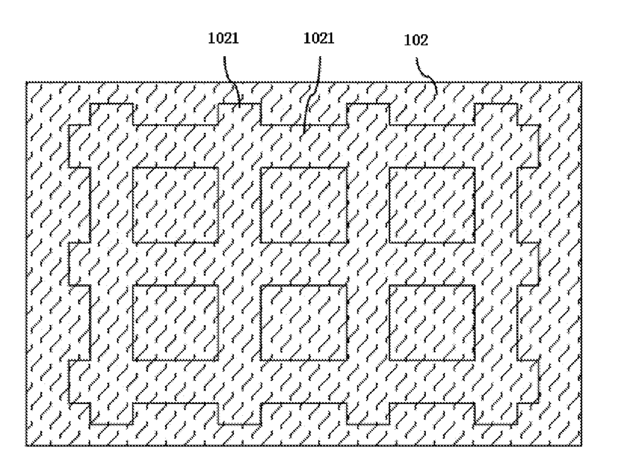
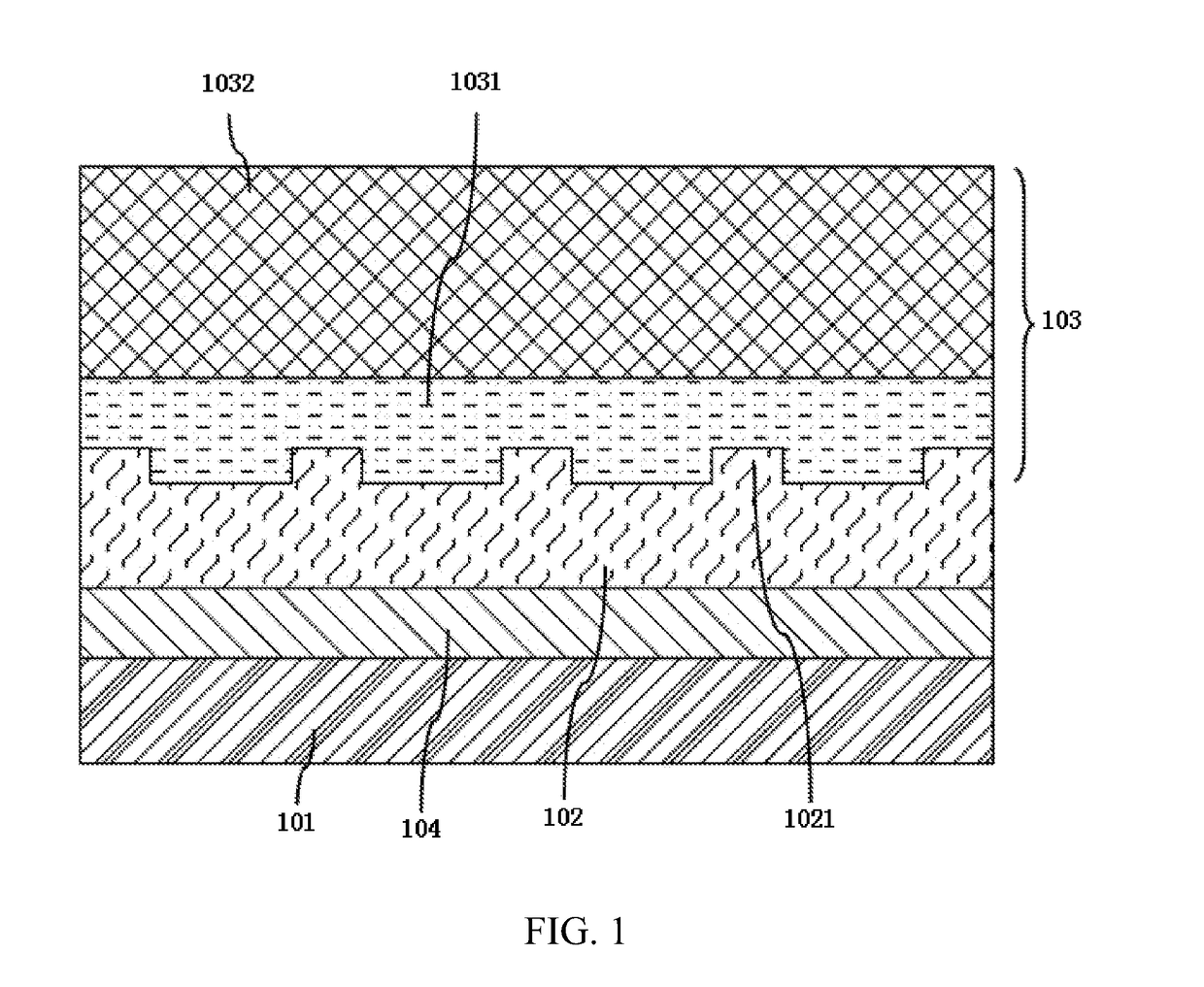
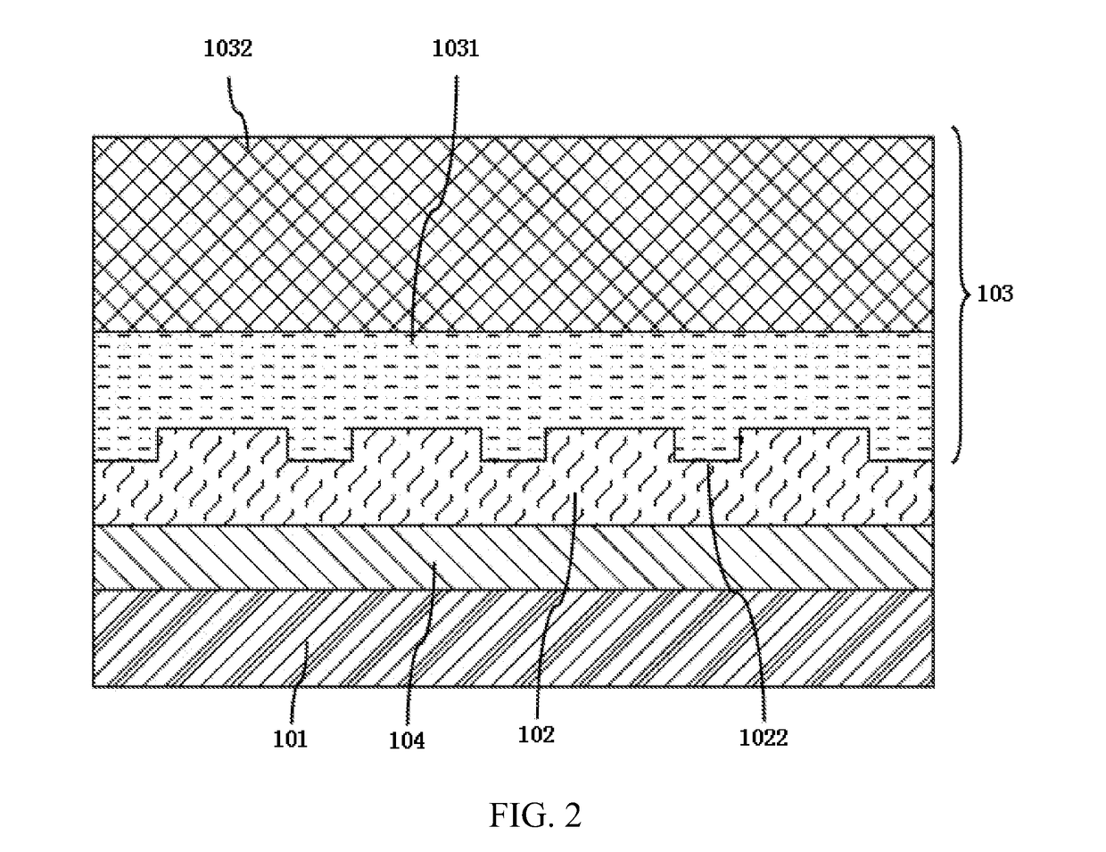
[0039]Refer to FIGS. 1-7. FIG. 1 is an illustrative drawing of a first preferred embodiment of a TFT array panel according to the present invention. FIG. 2 is an illustrative drawing of a second preferred embodiment of a TFT...


PUM


Abstract

The present invention provides a thin-film-transistor (TFT) array panel and manufacturing method of the same. The TFT array panel comprises a flexible baseplate, a buffer layer, and a display-element layer. The buffer layer is disposed on the flexible baseplate, a stress-elimination portion is disposed on the buffer layer, the stress-elimination portion is used to eliminate a stress of the flexible baseplate; the display-element layer is disposed on the buffer layer. The present invention is able to decrease the stress of the flexible baseplate, to prevent too large of a stress of the flexible baseplate.

Description

BACKGROUND OF THE INVENTION[0001]Field of Invention[0002]The present invention relates to the field of display driving technology, and more particularly to a thin-film-transistor (TFT) array panel and method of manufacturing the same.[0003]Description of Prior Art[0004]Conventional flexible displays generally comprise flexible baseplates, the flexible baseplates are generally too thin to perform corresponding processes directly on themselves, and hence, generally, the conventional flexible displays need to be fixed on glass baseplates, in order to perform the corresponding processes.[0005]In practice, the inventor has found that the conventional art at least the following problems:[0006]Because expansion coefficients of the glass baseplate and the flexible baseplate are different, there will be a warpage / bending phenomenon of glass substrate during the manufacturing process of the flexible substrate, which is not beneficial to the manufacturing process of the flexible substrate.[000...

Claims


Application Information

Patent Timeline
IPC IPC(8): H01L27/12H01L51/52H01L27/32
CPCH01L27/1218H01L27/1288H01L27/3272G02F1/1362H01L2251/5338H01L2227/323H01L51/52H01L21/77H01L27/1214H01L27/1259H01L2021/775H10K59/80G02F1/133305G02F2201/07H01L27/1262H10K50/80H10K59/126H10K59/1201H10K2102/311
Inventor HU, GUOREN
Owner TCL CHINA STAR OPTOELECTRONICS TECH CO LTD
Why Eureka
Try Eureka