Unlock instant, AI-driven research and patent intelligence for your innovation.

Voltage compensating circuit and voltage compensating method based on the voltage compensating circuit

a voltage compensating circuit and voltage compensating circuit technology, applied in the direction of instruments, static indicating devices, etc., can solve the problems of reducing the display effect of the liquid crystal display screen, reducing the display quality, and reducing the panel frame and product cost, so as to increase the display effect of the screen

Active Publication Date: 2017-06-08
TCL CHINA STAR OPTOELECTRONICS TECH CO LTD
View PDF2 Cites 10 Cited by
  • Summary
  • Abstract
  • Description
  • Claims
  • Application Information

AI Technical Summary

Benefits of technology

The present invention provides a voltage compensating circuit and a voltage compensating method for adjusting the voltage variation of the display in an active matrix liquid crystal display. The circuit detects the voltage variation of the thin film transistor and adjusts the gate driving signal accordingly, in real-time, to increase the display effect of the screen. The technical effect of this invention is to improve the display quality of the liquid crystal display by reducing the effect of temperature variation on the display performance.

Problems solved by technology

By using GOA technology, it may decrease the panel frame and the product cost.
When the TFT temperature varies, the electron mobility of the TFT drifts with the variation of the temperature, such that the gate scan driving signal of the TFT fluctuates, and then the grayscale of the liquid crystal display may be non-uniform, and the display quality is decreased.
However, since the substrate temperature detected by the temperature sensor is inconsistent with the actual temperature of the TFT in GOA circuit inside the substrate, the substrate temperature detected by the external temperature sensor can not accurately reflect the actual temperature of the TFT in GOA circuit inside the substrate, such that overcompensation or undercompensation of the gate scan driving voltage of the TFT occurs, thereby decreasing the display effect of the screen of the liquid crystal display.

Method used


Image

  • Voltage compensating circuit and voltage compensating method based on the voltage compensating circuit
  • Voltage compensating circuit and voltage compensating method based on the voltage compensating circuit
  • Voltage compensating circuit and voltage compensating method based on the voltage compensating circuit

Examples


Embodiment Construction

[0034]The present invention will now be combined with the implementation of the drawings, where a clear example of the technical solutions of the present invention, a complete description of, obviously, the described embodiments are only part of the embodiments of the present invention, but not all embodiments. Based on the embodiments of the present invention, all other embodiments obtained by those of ordinary skill without the creative work are within the scope of protection of the present invention.

[0035]An embodiment of the present invention provides a voltage compensating circuit and a voltage compensating method based on the voltage compensating circuit, thereby solving the problem of the variation of the substrate temperature which results in decreasing the display effect of the screen of the liquid crystal display. The descriptions are illustrated in details as following.

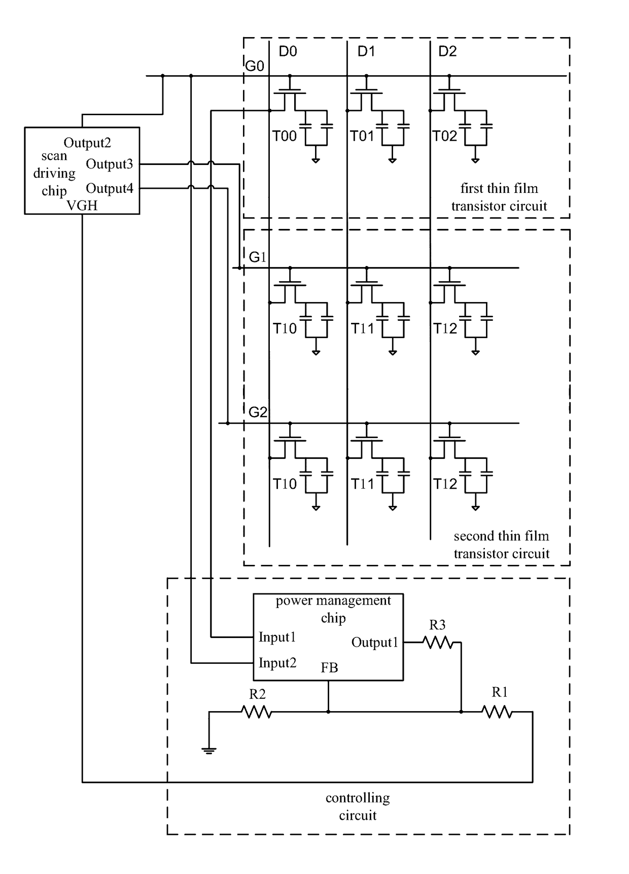
[0036]Please refer to FIG. 1. FIG. 1 is a voltage compensating circuit according to an embodiment of pre...


PUM


Abstract

A voltage compensating circuit and a method thereof are disclosed. The circuit includes a first TFT circuit, a controlling circuit and a scan driving chip. An output terminal of the power management chip of the controlling circuit connects to a first terminal of the third resistor, a second terminal of the third resistor connects to a first terminal of the first resistor, the second terminal of the third resistor connects to a feedback terminal of the chip, the feedback terminal of the chip connects to a first terminal of the second resistor, a second terminal of the second resistor connects to a ground, a second terminal of the first resistor connects to an input terminal of the scan driving chip. A source of the first TFT connects to a first input terminal of the chip, a second input terminal of the chip connects to the first gate driving signal.

Description

CROSS REFERENCE[0001]This application claims the benefit of Chinese Patent Application No. 201510425554.0, filed Jul. 17, 2015, titled “Voltage Compensating Circuit And Voltage Compensating Method Based On The Compensating Circuit”, the entire contents of which are incorporated by reference herein in its entirety.FIELD OF THE INVENTION[0002]The disclosure is related to liquid crystal display technology field, and more particular to a voltage compensating circuit and a voltage compensating method based on the voltage compensating circuit.BACKGROUND OF THE INVENTION[0003]In the active matrix liquid crystal display (AM-LCD), each pixel has a thin film transistor (TFT), which may adjust the brightness of each pixel independently, thereby increasing the display effect of the liquid crystal display. A gate on array (GOA) technology is generally used in AM-LCD. GOA technology is a technology for manufacturing the gate scan driving circuit of TFT on a substrate. By using GOA technology, it ...

Claims


Application Information

Patent Timeline
Patent Type & Authority Applications(United States)
IPC IPC(8): G09G3/36
CPCG09G3/3696G09G3/3677G09G2300/043G09G2320/0666G09G2320/0646G09G2320/041G09G2330/00G09G2300/0408
Inventor XIONG, ZHI
Owner TCL CHINA STAR OPTOELECTRONICS TECH CO LTD