Package substrate and manufacturing method thereof, and OLED display device

a technology of packaging substrate and manufacturing method, applied in the field of display technology, can solve the problems of display fault and affect the service life of the display device, and achieve the effect of improving the package effect of the oled device and preventing the introduction of water and oxygen

Inactive Publication Date: 2017-06-22
BOE TECH GRP CO LTD +1
View PDF13 Cites 8 Cited by
  • Summary
  • Abstract
  • Description
  • Claims
  • Application Information

AI Technical Summary

Benefits of technology

[0017]According to the embodiments of the present invention, by providing the concave-convex structures at the corners of the package substrate, frosted surfaces are formed at the corners of the package substrate, so that a contact area between the sealant and the package substrate can be effectively increased after the package substrate and the base substrate are laminated together, and intrusion of water and oxygen is prevented, thereby improving package effect of the OLED device.

Problems solved by technology

If intrusion of water and oxygen occurs, it is very likely to cause dark spots in a light-emitting region, which will result in display fault and affect service life of the display device.

Method used


Image

  • Package substrate and manufacturing method thereof, and OLED display device
  • Package substrate and manufacturing method thereof, and OLED display device
  • Package substrate and manufacturing method thereof, and OLED display device

Examples


Embodiment Construction

[0028]Embodiments of the present invention will be described clearly and completely below with reference to the accompanying drawings. However, the described embodiments are just for illustration, but not intended to limit the scope of the present invention.

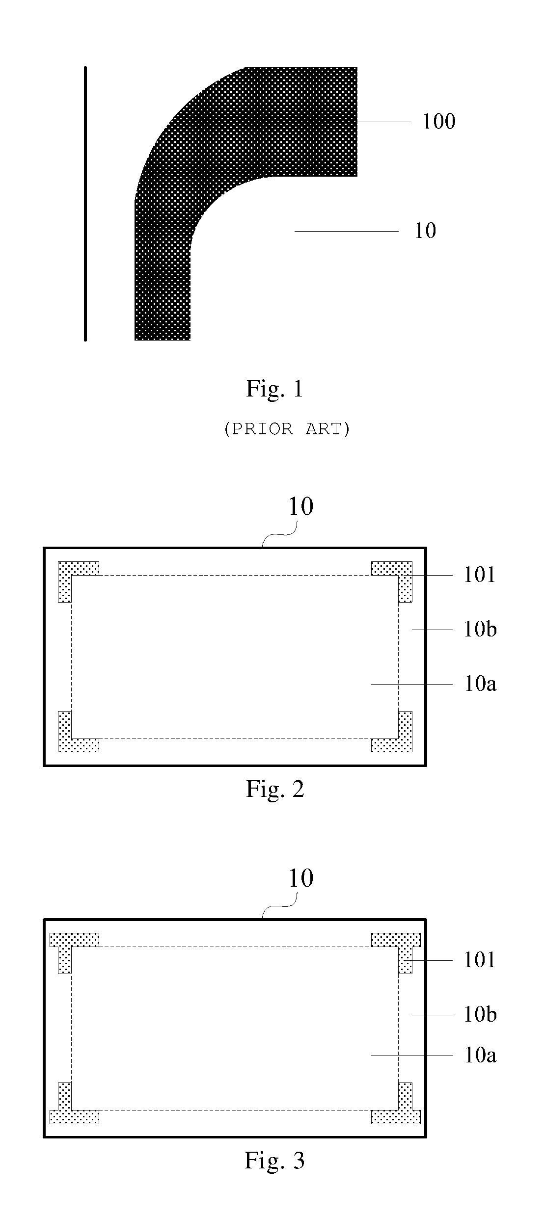
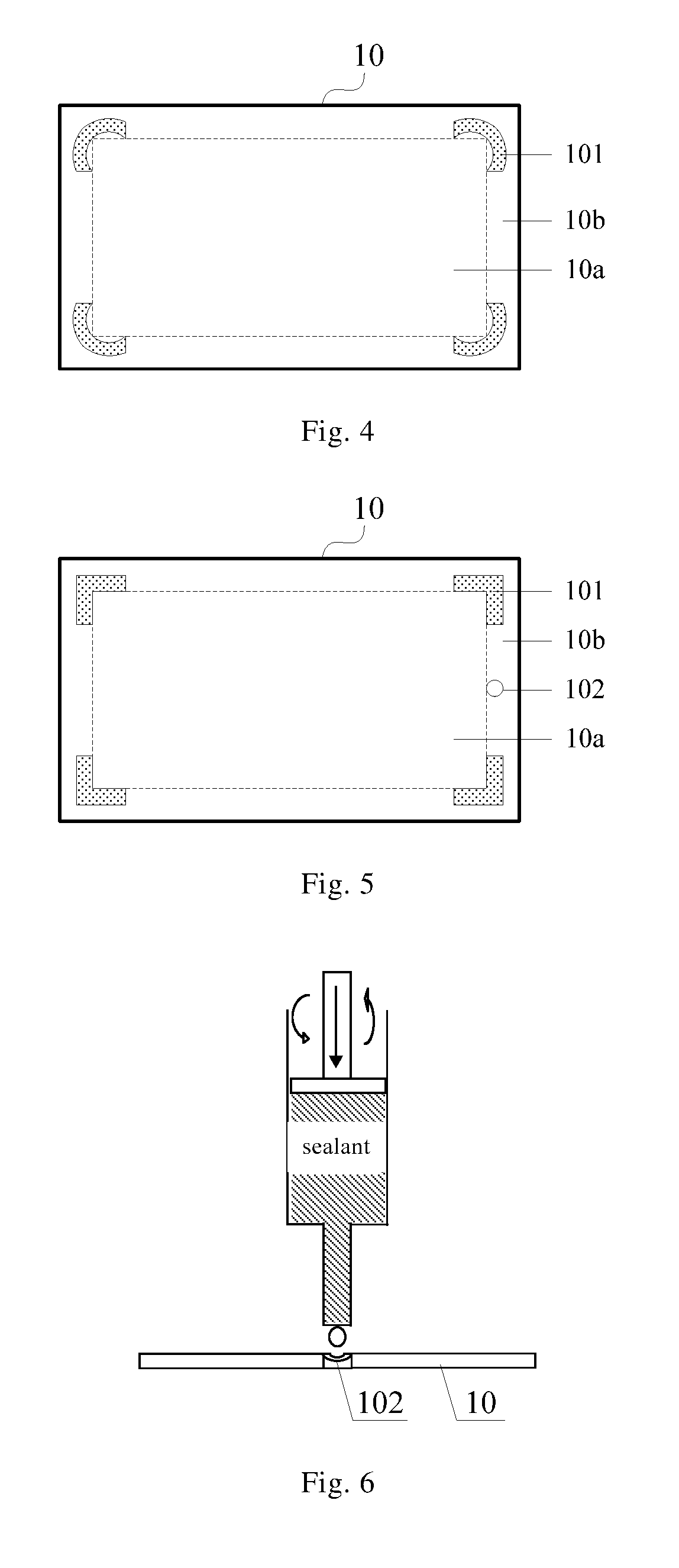
[0029]FIGS. 2-4 are schematic structural diagrams of package substrates according to the embodiments of the present invention.

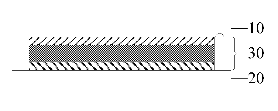
[0030]With reference to FIGS. 2-4, a package substrate 10 according to the embodiments of the present invention comprises a central region 10a used for being coated with filler adhesive, and a peripheral region 10b used for being coated with sealant. Surface of the peripheral region 10b at each corner thereof includes a concave-convex structure 101.

[0031]The package substrate 10 can be used for packaging an OLED device. According to different light exiting directions of OLED devices, the package substrate 10 may be a transparent substrate (e.g. a glass substrate) or an opaque substrate (e.g. a metal substr...


PUM


Abstract

Embodiments of the present invention provide a package substrate and a manufacturing method thereof. The package substrate (10) comprises a central region (10a) used for being coated with filler adhesive, and a peripheral region (10b) used for being coated with sealant. Surface of the peripheral region (10b) at corners thereof includes concave-convex structures (101). The present invention further provides an OLED display device comprising the package substrate (10).

Description

FIELD OF THE INVENTION[0001]The present invention relates to the field of display technology, and particularly relates to a package substrate and a manufacturing method thereof, and an OLED display device comprising the package substrate.BACKGROUND OF THE INVENTION[0002]Due to the advantages of self-illumination, high brightness, fast response speed, light weight and thinness, full color and no parallax, organic light emitting display (OLED) devices have been applied in display field.[0003]An organic material functional layer in an OLED device is particularly sensitive to water vapor and oxygen. If intrusion of water and oxygen occurs, it is very likely to cause dark spots in a light-emitting region, which will result in display fault and affect service life of the display device.[0004]With respect to an OLED device formed on a glass substrate, glass package is mainly adopted in the prior art. For example, after an OLED device is formed on a base substrate, a package substrate may b...

Claims


Application Information

Patent Timeline
Patent Type & Authority Applications(United States)
IPC IPC(8): H01L51/52H01L51/56
CPCH01L51/56H01L51/5246H10K50/841H10K50/8426H10K71/00
Inventor QUAN, WEICHANG, CHIA HAO
Owner BOE TECH GRP CO LTD
Why Eureka
Try Eureka