Supercharge Your Innovation With Domain-Expert AI Agents!

OLED gate driving circuit structure

Active Publication Date: 2017-06-29
TCL CHINA STAR OPTOELECTRONICS TECH CO LTD
View PDF6 Cites 3 Cited by
  • Summary
  • Abstract
  • Description
  • Claims
  • Application Information

AI Technical Summary

Benefits of technology

The present invention provides an OLED gate driving circuit structure using only one gate driving integrated circuit for achieving the charge and discharge procedures of the gate driving circuit. This saves hardware costs and simplifies the panel layout circuit, making the frame of the panel narrower. The effect of this invention is to provide a more efficient and economical OLED panel design.

Problems solved by technology

However, the aforesaid OLED gate driving circuit structure requires two gate driving ICs and the hardware cost is high; meanwhile, the peripheral circuit of the OLED panel is added so that the frame of the panel becomes wider, which increases the technical requirements and the cost.

Method used


Image

  • OLED gate driving circuit structure
  • OLED gate driving circuit structure
  • OLED gate driving circuit structure

Examples


Embodiment Construction

[0074]For better explaining the technical solution and the effect of the present invention, the present invention will be further described in detail with the accompanying drawings and the specific embodiments.

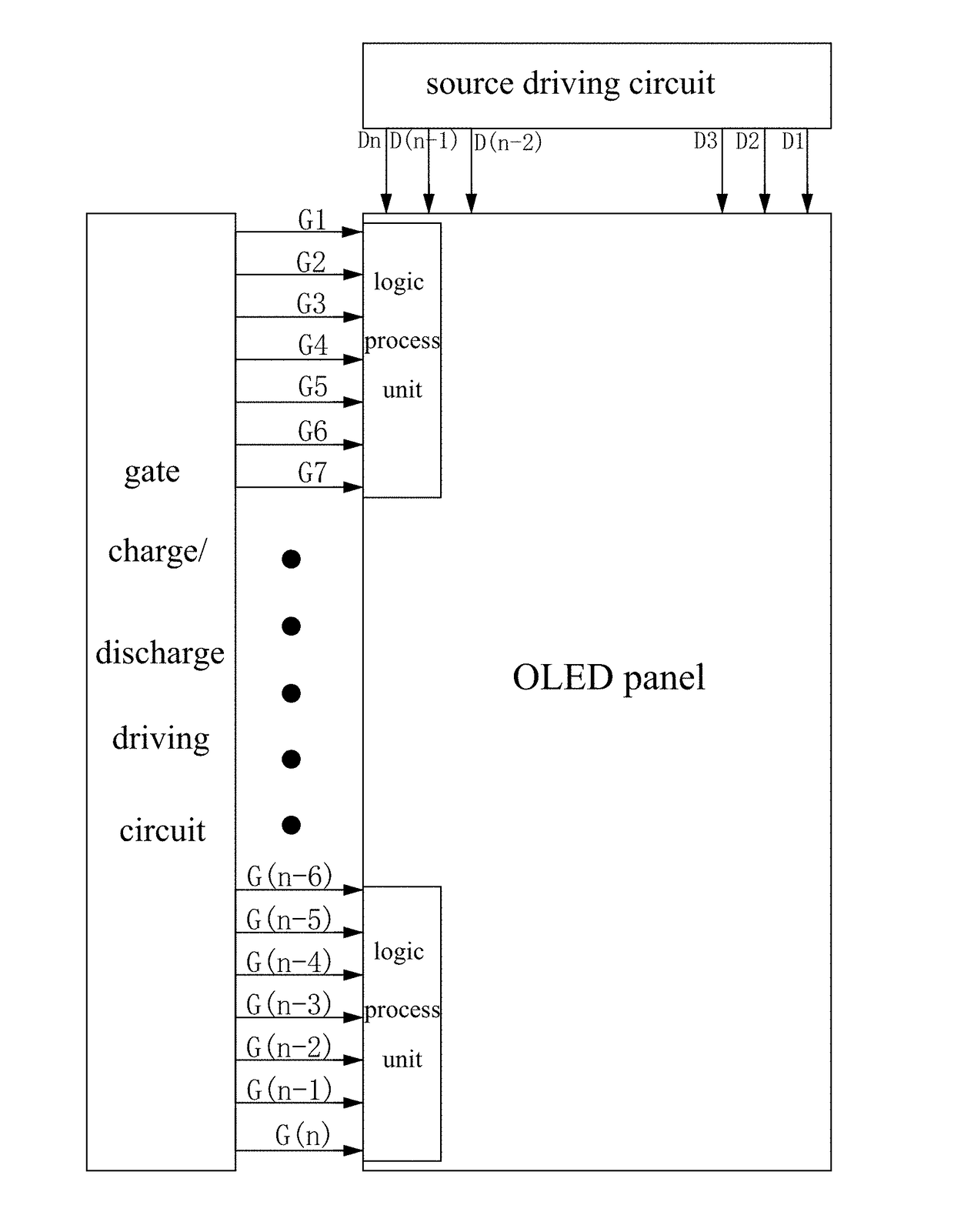
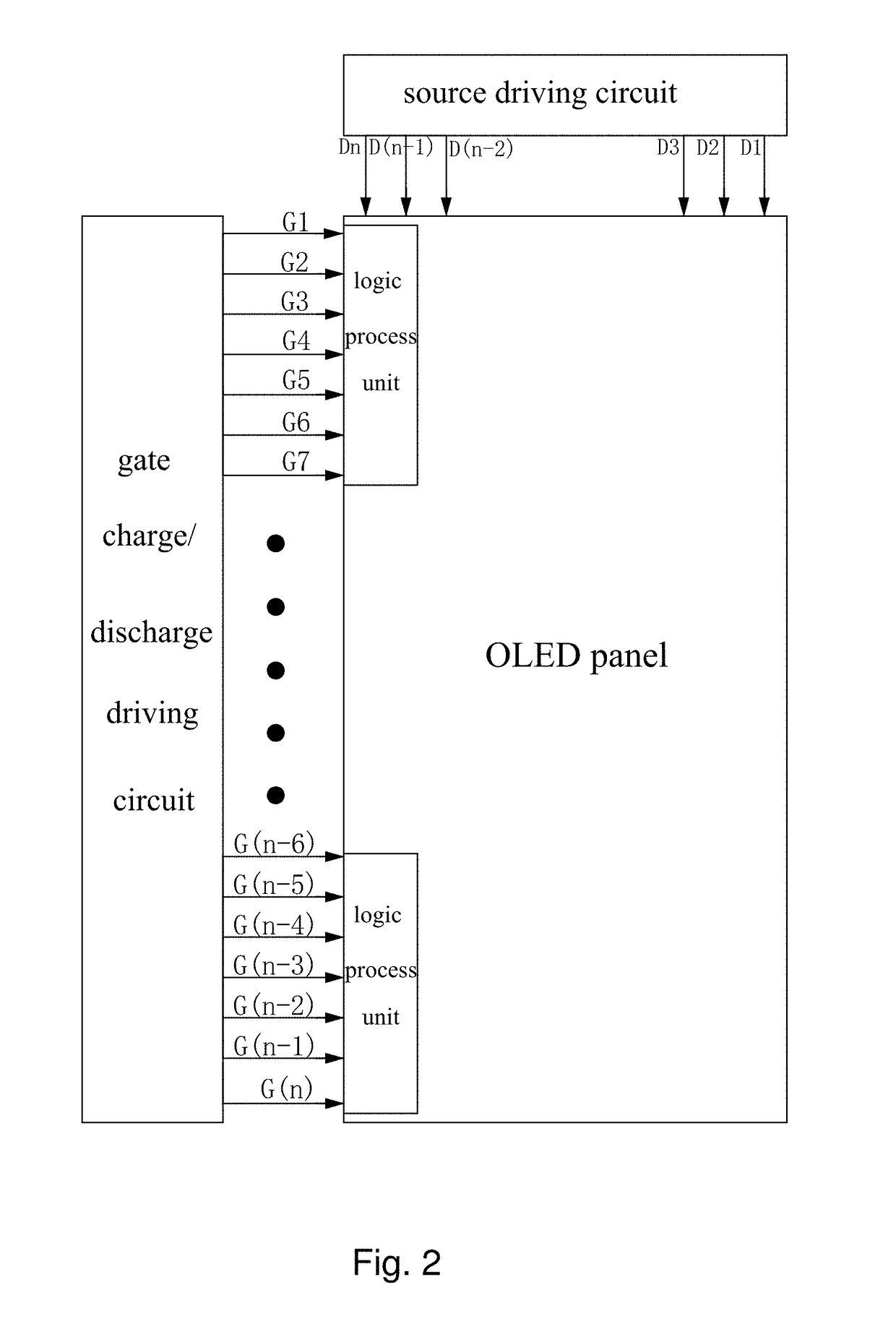
[0075]Please refer to FIG. 2. The present invention provides an OLED gate driving circuit structure, comprising: an OLED panel, a gate charge / discharge driving circuit, a logic process unit and a source driving circuit; the gate charge / discharge driving circuit is located at one side of the OLED panel, and the gate charge / discharge driving circuit comprises a plurality of output ends, and each output end is electrically coupled to the logic process unit with one signal line; the logic process unit is located inside the OLED panel, and the logic process unit receives a scan signal transmitted by the gate charge / discharge driving circuit through the signal line, and converts the scan signal into a discharge scan signal and a charge scan signal to be provided to the OLED panel; t...


PUM


Abstract

The present invention provides an OLED gate driving circuit structure, comprising an OLED panel, a gate charge / discharge driving circuit, a logic process unit and a source driving circuit; the gate charge / discharge driving circuit is located at one side of the OLED panel, and the gate charge / discharge driving circuit comprises a plurality of output ends, and each output end is electrically coupled to the logic process unit with one signal line; the logic process unit is located inside the OLED panel, and the logic process unit receives a scan signal transmitted by the gate charge / discharge driving circuit through the signal line, and converts the scan signal into a discharge scan signal and a charge scan signal to be provided to the OLED panel; the source driving circuit is coupled to the OLED panel, and provides a data signal to the OLED panel, and only one gate driving integrated circuit is utilized in the structure for achieving the charge and discharge procedures of the gate driving circuit to save the hardware cost and to simplify the panel layout circuit and to make the frame of the panel narrower.

Description

FIELD OF THE INVENTION[0001]The present invention relates to a display technology field, and more particularly to an OLED gate driving circuit structure.BACKGROUND OF THE INVENTION[0002]The Organic Light Emitting Display (OLED) possesses many outstanding properties of self-illumination, low driving voltage, high luminescence efficiency, short response time, high clarity and contrast, near 180° view angle, wide range of working temperature, applicability of flexible display and large scale full color display. The OLED is considered as the most potential display device.[0003]The OLED can be categorized into two major types according to the driving methods, which are the Passive Matrix OLED (PMOLED) and the Active Matrix OLED (AMOLED), i.e. two types of the direct addressing and the Thin Film Transistor (TFT) matrix addressing. The AMOLED comprises pixels arranged in array and belongs to active display type, which has high lighting efficiency and is generally utilized for the large sca...

Claims


Application Information

Patent Timeline
IPC IPC(8): G09G3/3266G09G3/3275G09G3/3225
CPCG09G3/3266G09G3/3225G09G2310/0243G09G2310/0291G09G2310/08G09G3/3275
Inventor KUANG, JIMUWU, CHIHHAOHU, HOULIANG
Owner TCL CHINA STAR OPTOELECTRONICS TECH CO LTD
Features
  • R&D
  • Intellectual Property
  • Life Sciences
  • Materials
  • Tech Scout
  • Unparalleled Data Quality
  • Higher Quality Content
  • 60% Fewer Hallucinations
Learn More