Pixel structure

a pixel and structure technology, applied in the field of pixel structure, can solve the problems of low aperture ratio, reduced pixel size, and increased difficulty in wiring design of pixels, and achieve the effect of high aperture ratio

Active Publication Date: 2017-07-06
AU OPTRONICS CORP
View PDF4 Cites 3 Cited by
  • Summary
  • Abstract
  • Description
  • Claims
  • Application Information

AI Technical Summary

Benefits of technology

[0005]The present invention provides a pixel structure having a high aperture ratio.

Problems solved by technology

Particularly, in order to achieve a high resolution, it is necessary to deploy more pixels in the same area, so that the size of the pixel is becoming smaller and smaller, and the wiring design of the pixels will be faced with more stringent challenges.
However, when the above wiring manner is implemented in connection with a fabricating manner of color Filter on Array (COA), low aperture ratio often results.

Method used


Image

  • Pixel structure
  • Pixel structure
  • Pixel structure

Examples


Embodiment Construction

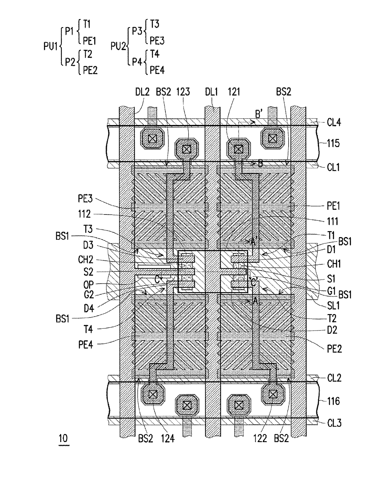
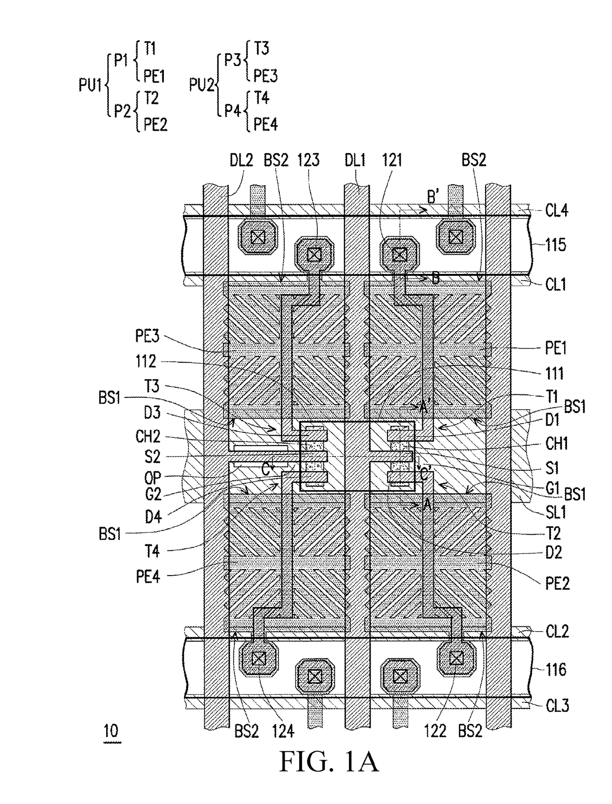
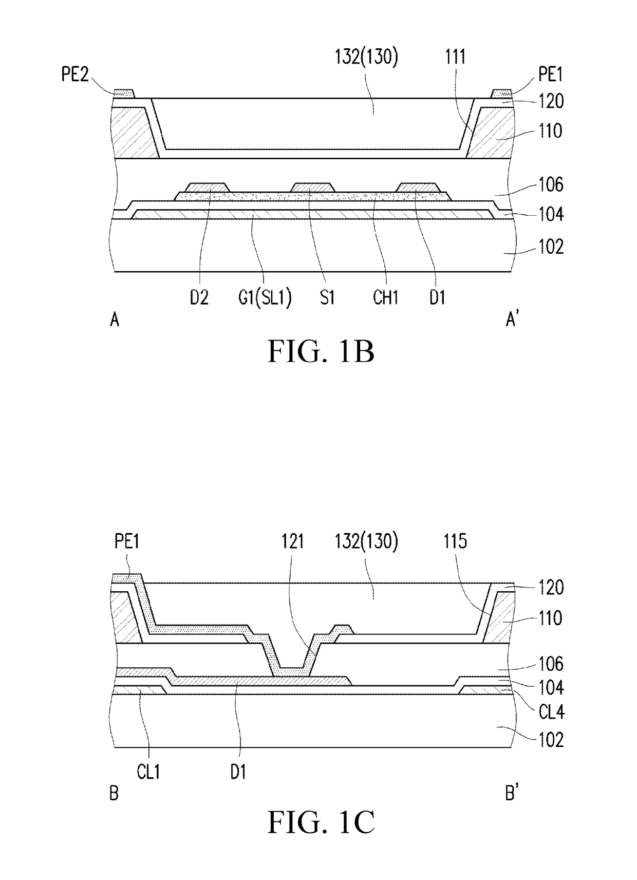
[0041]FIG. 1A is a schematic view of a pixel structure according to an embodiment of the present invention. FIG. 1B to FIG. 1D are respectively schematic cross-sectional views along the lines A-A′, B-B′, and C-C′ in FIG. 1A. With reference to FIG. 1A to FIG. 1D altogether, a pixel structure 10 includes a first scan line SL1, a first data line DL1, a first common line CL1, a second common line CL2, a first pixel unit PU1, a color filter layer 110, and a shielding pattern layer 130 arranged on a substrate 102. The first data line DL1 intersects with the first scan line SL1. The first scan line SL1 is disposed between the first common line CL1 and the second common line CL2.

[0042]The first pixel unit PU1 includes a first sub-pixel P1 and a second sub-pixel P2. The first sub-pixel P1 includes a first active device T1 and a first pixel electrode PE1. The first active device T1 is electrically connected to the first scan line SL1 and the first data line DL1. The first pixel electrode PE1 ...


PUM


Abstract

A pixel structure includes a scan line, a data line, first and second common lines, first and second sub-pixels, and a color filter layer. The scan line is disposed between the first and second common lines. The first sub-pixel and the second pixel respectively include an active device and a pixel electrode. The pixel electrode of the first sub-pixel is disposed between the scan line and the first common line. The pixel electrode of the second sub-pixel is disposed between the scan line and the second common line. The pixel electrode is connected to the active device through a contact hole. The pixel electrode includes a first side and a second side opposite to each other, wherein the first side of the pixel electrode is adjacent to the scan line, and the contact hole is disposed at an edge of the pixel electrode adjacent to the second side. The color filter layer has an opening exposing the active devices of the first sub-pixel and the second sub-pixel.

Description

BACKGROUND[0001]The present application claims priority to Taiwan patent application 105100096, filed Jan. 4, 2016, the contents of which are incorporated herein by reference.TECHNICAL FIELD[0002]The present invention relates to a pixel structure, and in particular, to a pixel structure adapted to have a small size.RELATED ART[0003]Along with the development of display technologies, the requirements on the display panel are also developed to become lighter and thinner, having a high picture quality, and saving power. Particularly, in order to achieve a high resolution, it is necessary to deploy more pixels in the same area, so that the size of the pixel is becoming smaller and smaller, and the wiring design of the pixels will be faced with more stringent challenges.[0004]Generally speaking, the manner of providing two common lines having different electric potentials to respectively couple with a storage capacitance of a major sub-pixel region and an auxiliary sub-pixel region in th...

Claims


Application Information

Patent Timeline
Patent Type & Authority Applications(United States)
IPC IPC(8): G09G3/36
CPCG09G3/3607G09G3/3674G09G2300/0443G09G2300/0426G09G2300/0452G09G2320/0666G02F1/1362G02F1/136209G02F1/136227G02F1/136286G02F1/136222
Inventor HO, SHENG-JUHUANG, MENG-CHIOUPAI, CHIA-HUIWU, SHANG-JIECHEN, YI-JUNGLIN, HUNG-CHE
Owner AU OPTRONICS CORP
Why Eureka
Try Eureka