
Light source module, display panel, display apparatus and methods for manufacturing the same

a technology of light source modules and display panels, which is applied in the direction of electric lighting sources, solid-state devices, and light source components, etc., can solve the problem of difficult implementation of target color coordinates in led display panels

Active Publication Date: 2017-08-17
SAMSUNG ELECTRONICS CO LTD
View PDF5 Cites 102 Cited by
  • Summary
  • Abstract
  • Description
  • Claims
  • Application Information

AI Technical Summary

Benefits of technology

The patent text describes an LED sub-pixel, an LED pixel comprising multiple sub-pixels, and a display panel or other display device using these sub-pixels. The sub-pixels have a tuning phosphor that absorbs light emitted by the LED and emits light at a different wavelength, resulting in improved color characteristics. The method of manufacturing involves forming the sub-pixels on a semiconductor wafer and then singulating them to create a semiconductor chip. The chip can then be used to create a display panel or other display device. The technical effects include improved color accuracy and reduced power consumption.

Problems solved by technology

However, there is a problem in that target color coordinates are difficult to implement in such LED display panels due to variations in optical characteristics (e.g. peak wavelength or luminance characteristics) of LED chips forming the sub-pixels.

Method used


Image

  • Light source module, display panel, display apparatus and methods for manufacturing the same
  • Light source module, display panel, display apparatus and methods for manufacturing the same
  • Light source module, display panel, display apparatus and methods for manufacturing the same

Examples


Embodiment Construction

[0037]The present disclosure now will be described more fully hereinafter with reference to the accompanying drawings, in which various embodiments are shown. The invention may, however, be embodied in many different forms and should not be construed as limited to the example embodiments set forth herein. These example embodiments are just that—examples—and many implementations and variations are possible that do not require the details provided herein. It should also be emphasized that the disclosure provides details of alternative examples, but such listing of alternatives is not exhaustive. Furthermore, any consistency of detail between various examples should not be interpreted as requiring such detail—it is impracticable to list every possible variation for every feature described herein. The language of the claims should be referenced in determining the requirements of the invention.

[0038]Throughout the specification, it will be understood that when an element, such as a layer...


PUM


Abstract

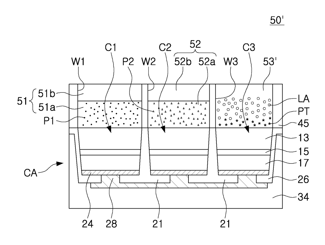
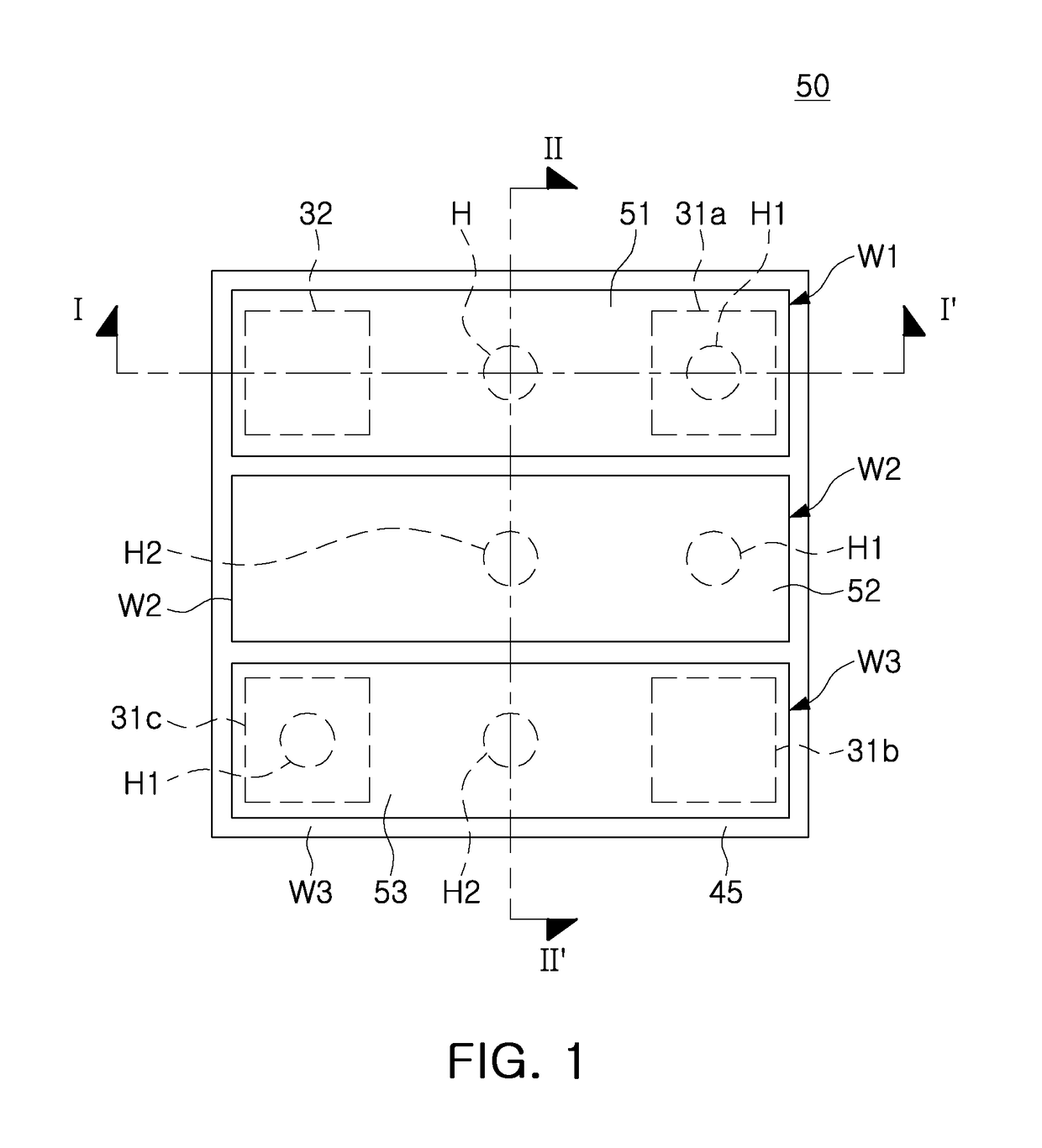
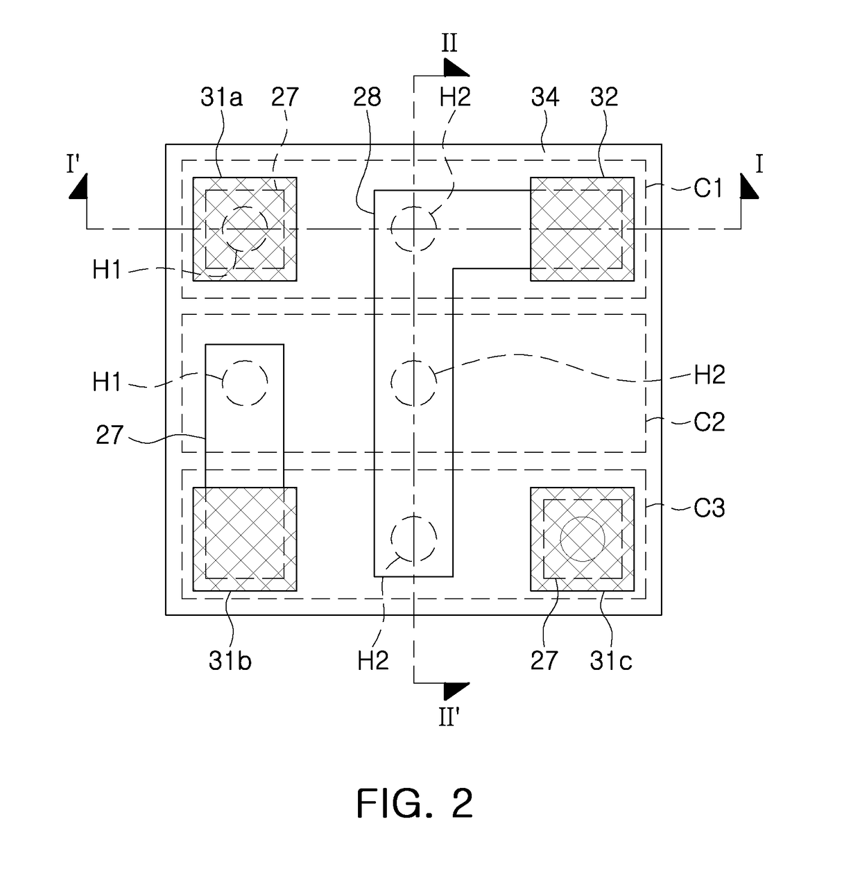
A pixel of a light emitting diode module, display panel or other device, may comprise different colored sub-pixels, where one of the sub-pixels comprises a wavelength converting material, such as phosphor, to convert light emitted from an associated light emitting diode of that sub-pixel into a color other than the main color of light emitted from that sub-pixel. The wavelength converting material may have an amount selected to tune the color coordinates of the pixel. The amount of wavelength converting material may be determined in response to measuring the intensity of the spectrum of light emitted by the light emitting diode of the sub-pixel, or similarly manufactured sub-pixels, on which the wavelength converting material is to be formed. Methods of manufacturing the same are also disclosed.

Description

CROSS-REFERENCE TO RELATED APPLICATION[0001]This application claims the priority and benefit of Korean Patent Application No. 10-2016-0016055, filed on Feb. 12, 2016, with the Korean Intellectual Property Office, the entire contents of which is incorporated herein by reference.BACKGROUND[0002]1. Field[0003]The inventive concept relates to a light source module, a display panel, and a display device.[0004]2. Description of Related Art[0005]Semiconductor light emitting diodes (LEDs) have been used as light sources in various electronic products, as well as light sources in lighting devices. In particular, semiconductor LED devices are being widely used as light sources in various display devices, such as TVs, mobile phones, PCs, laptop PCs, and PDAs.[0006]Display devices commonly include display panels, such as liquid crystal display (LCD) panels, and backlights. However, recently, display devices using an LED device as a single pixel that do not require use of a backlight have been b...

Claims


Application Information

Patent Timeline
IPC IPC(8): H01L27/15H01L33/50H05B44/00
CPCH01L27/156H01L33/502H01L2933/0041H05B33/0845H05B37/0272H01L33/505H01L27/153H01L33/48H05B45/20H05B47/195H05B47/19H01L25/0753H01L25/167H01L33/0095H01L33/44H01L33/504
Inventor LEE, JIN SUBSEONG, HAN KYUKIM, YONG ILKIM, JUNG SUBLEE, SEUL GEE
Owner SAMSUNG ELECTRONICS CO LTD
Learn More