Memory device and method of manufacturing the same

a memory device and manufacturing method technology, applied in the field of memory devices, can solve the problems of reducing productivity and reducing and achieve the effect of enhancing the reliability of memory devices

Active Publication Date: 2017-08-24
SAMSUNG ELECTRONICS CO LTD
View PDF0 Cites 37 Cited by
  • Summary
  • Abstract
  • Description
  • Claims
  • Application Information

AI Technical Summary

Benefits of technology

[0004]Embodiments of the inventive concept provides a memory device and a method of manufacturing the same, in which a defect caused by a process of patterning a memory cell is minimized, thereby enhancing the reliability of the memory device.

Problems solved by technology

However, due to the miniaturization of the memory devices, various defects may occur in the process of manufacturing the memory devices, and the resulting defects may degrade the reliability of the memory devices and may reduce productivity.

Method used


Image

  • Memory device and method of manufacturing the same
  • Memory device and method of manufacturing the same
  • Memory device and method of manufacturing the same

Examples


Embodiment Construction

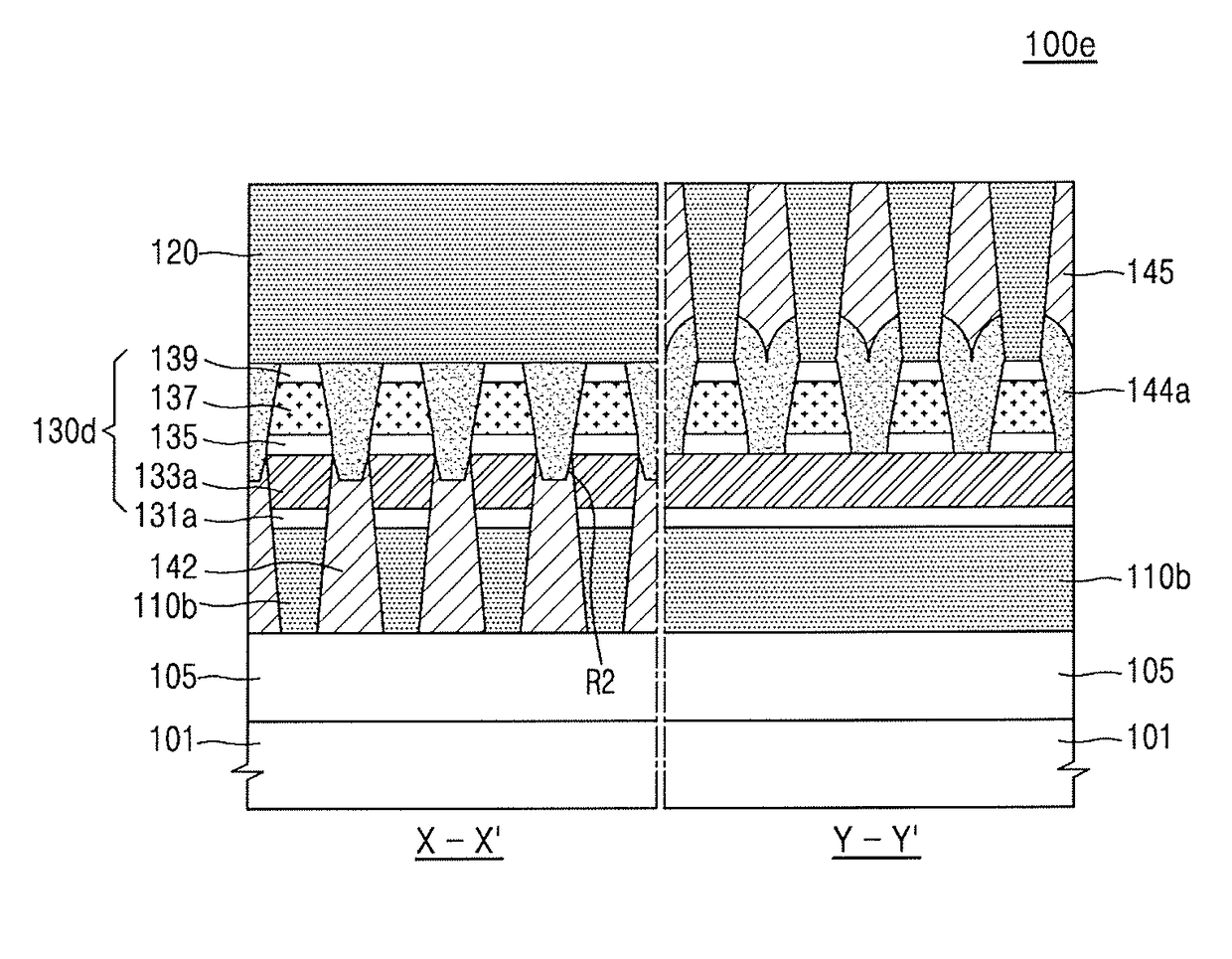
[0028]FIG. 1 is an equivalent circuit diagram of a memory device 100 according to an exemplary embodiment of the inventive concept.

[0029]Referring to FIG. 1, the memory device 100 may include a plurality of bottom word lines WL11 and WL12, which extend along a first direction (an X direction) and are spaced apart from each other in a second direction (a Y direction) perpendicular to the first direction, and a plurality of top word lines WL21 and WL22 that are spaced apart from each other in the second direction, are spaced apart from the bottom word lines WL11 and WL12 in a third direction (a Z direction) perpendicular to the first direction and the second direction, and extend along the first direction. Also, the memory device 100 may include a plurality of common bit lines BL1 to BL4 that are spaced apart from the top word lines WL21 and WL22 and the bottom word lines WL11 and WL12 in the third direction and extend along the second direction.

[0030]A first memory cell MC1 and a sec...


PUM


Abstract

Provided are a memory device and a method of manufacturing the same. Memory cells of the memory device are formed separately from first electrode lines and second electrode lines, wherein the second electrode lines over the memory cells are formed by a damascene process, thereby avoiding complications associated with CMP being excessively or insufficiently performed on an insulation layer over the memory cells.

Description

CROSS-REFERENCE TO RELATED APPLICATION[0001]This application claims the benefit under 35 U.S.C. §119 of Korean Patent Application No. 10-2016-0020696, filed on Feb. 22, 2016, in the Korean Intellectual Property Office, the disclosure of which is incorporated by reference herein in its entirety.TECHNICAL FIELD[0002]The inventive concept relates to a memory device and a method of manufacturing the same, and more particularly, to a memory device having a cross-point stacked structure and a method of manufacturing the same.DISCUSSION OF RELATED ART[0003]With the lightening, thinning, shortening and miniaturizing trend of electronic products, there is a growing demand for highly-integrated semiconductor devices. To meet this demand, memory devices having a three-dimensional (3D) cross-point stacked structure in which a memory cell is disposed at a cross point between two electrodes crossing each other have been proposed. In addition, to meet the continuous requirement of down-scaling the...

Claims


Application Information

Patent Timeline
Patent Type & Authority Applications(United States)
IPC IPC(8): H01L45/00H01L27/24
CPCH01L45/144H01L45/16H01L27/2463H01L45/126H10B63/80H10B63/84H10N70/821H10N70/826H10B63/24H10N70/20H10N70/8413H10N70/882H10N70/231H10N70/8828H10N70/063H10N70/066H10N70/011
Inventor JEONG, JI-HYUNLEE, JIN-WOOKOH, GWAN-HYEOBKANG, DAE-HWAN
Owner SAMSUNG ELECTRONICS CO LTD
Why Eureka
Try Eureka