Self-assembled monolayer blocking with intermittent air-water exposure

a monolayer and air-water exposure technology, applied in semiconductor/solid-state device manufacturing, basic electric elements, electric devices, etc., can solve the problems of increasing processing capacity, ineffectively preventing the deposition of subsequent material layers, and long time for deposition,

Active Publication Date: 2017-09-07
APPLIED MATERIALS INC
View PDF3 Cites 68 Cited by
  • Summary
  • Abstract
  • Description
  • Claims
  • Application Information

AI Technical Summary

Problems solved by technology

Reliably producing sub-half micron and smaller features is one of the key technology challenges for next generation very large scale integration (VLSI) and ultra large scale integration (ULSI) of semiconductor devices.
However, as the limits of circuit technology are pushed, the shrinking dimensions of VLSI and ULSI technology have placed additional demands on processing capabilities.
However, SAMs may exhibit pin holes or voids in as deposited layers which may not effectively prevent deposition of subsequent material layers.
Another drawback of SAMs is that the time for deposition may be very long and not economically feasible in semiconductor manufacturing processes.

Method used


Image

  • Self-assembled monolayer blocking with intermittent air-water exposure
  • Self-assembled monolayer blocking with intermittent air-water exposure
  • Self-assembled monolayer blocking with intermittent air-water exposure

Examples


Embodiment Construction

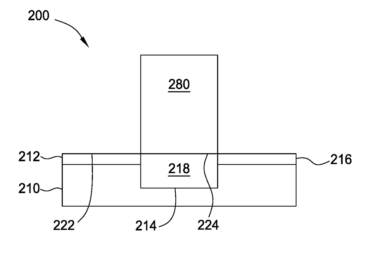
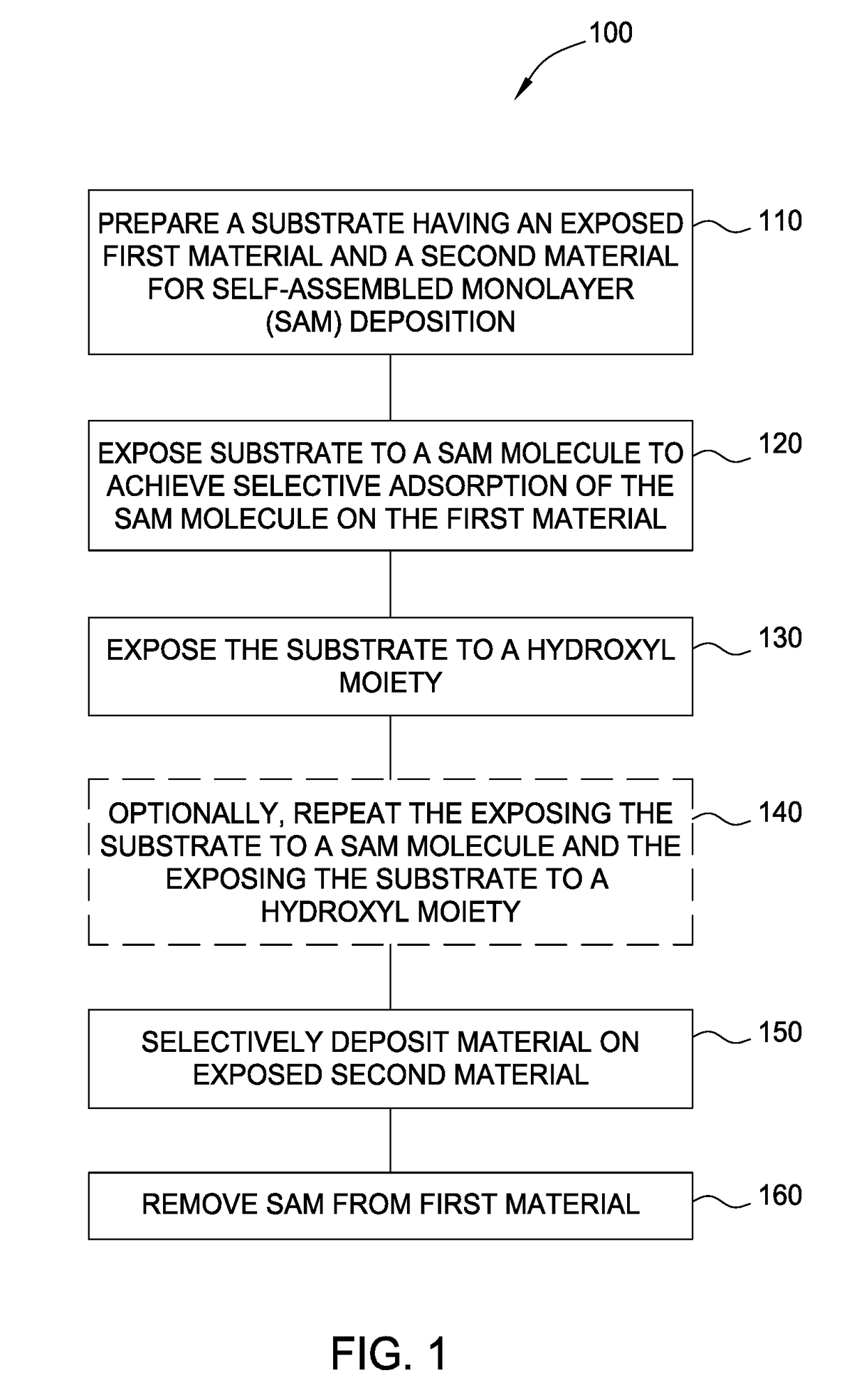
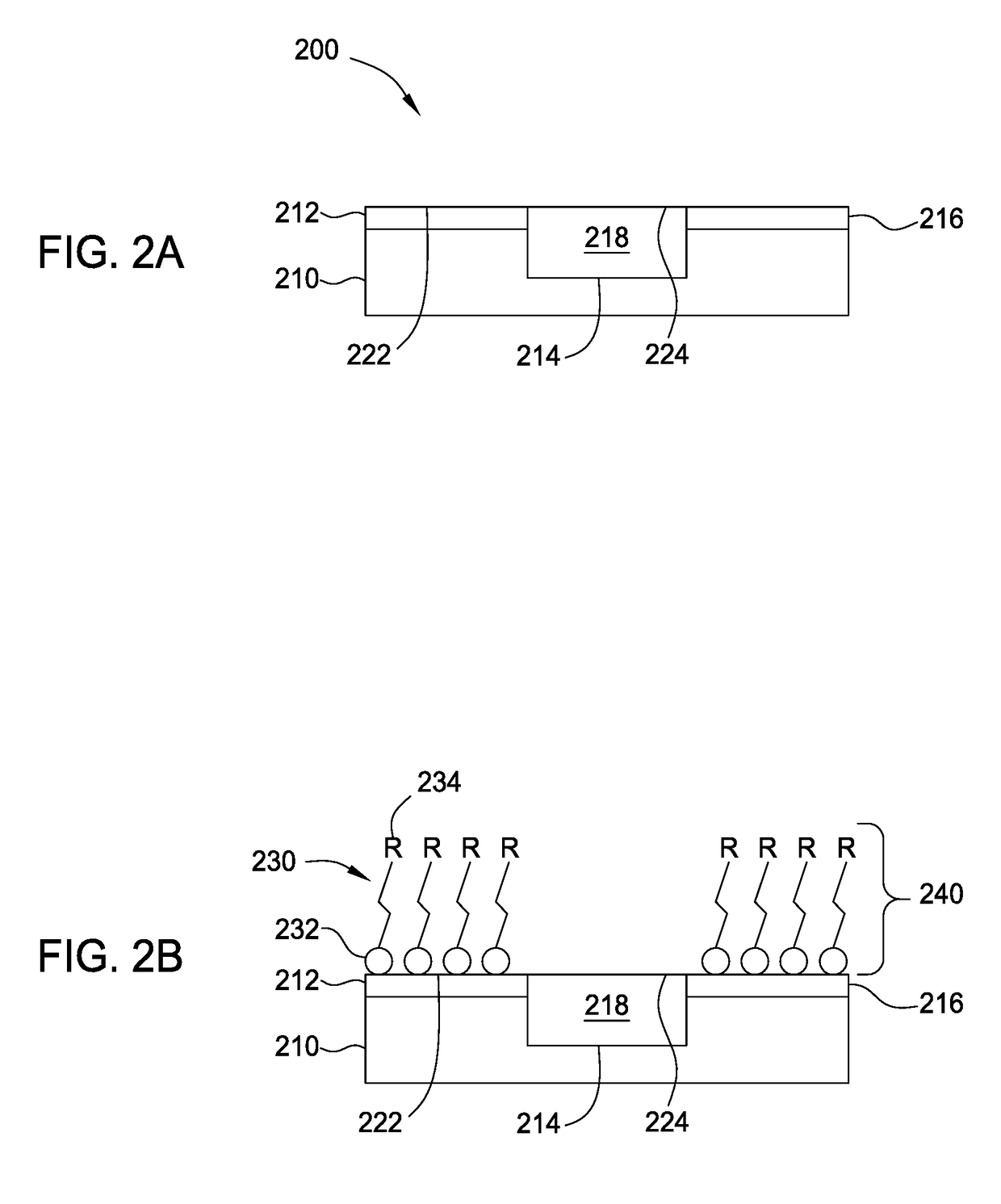
[0016]The following disclosure describes processes for the fabrication of semiconductor devices in which a self-assembled monolayer is used to achieve selective deposition. Certain details are set forth in the following description and in FIG. 1 and FIGS. 2A-2B, to provide a thorough understanding of various implementations of the disclosure. Other details describing structures and systems often associated with semiconductor devices and self-assembled monolayers are not set forth in the following disclosure to avoid unnecessarily obscuring the description of the various implementations.

[0017]Many of the details, dimensions, angles and other features shown in the Figures are merely illustrative of particular implementations. Accordingly, other implementations can have other details, components, and features without departing from the spirit or scope of the present disclosure. In addition, further implementations of the disclosure can be practiced without several of the details descri...


PUM


Abstract

Implementations described herein generally relate to processes for the fabrication of semiconductor devices in which a self-assembled monolayer (SAM) is used to achieve selective area deposition. Methods described herein relate to alternating SAM molecule and hydroxyl moiety exposure operations which may be utilized to form SAM layers suitable for blocking deposition of subsequently deposited materials.

Description

CROSS-REFERENCE TO RELATED APPLICATIONS[0001]This application claims benefit of U.S. Provisional Patent Application No. 62 / 303,069, filed Mar. 3, 2016, the entirety of which is herein incorporated by reference.BACKGROUND[0002]Field[0003]Implementations described herein generally relate to processes for the fabrication of semiconductor devices in which a self-assembled monolayer is used to achieve selective area deposition.[0004]Description of the Related Art[0005]Reliably producing sub-half micron and smaller features is one of the key technology challenges for next generation very large scale integration (VLSI) and ultra large scale integration (ULSI) of semiconductor devices. However, as the limits of circuit technology are pushed, the shrinking dimensions of VLSI and ULSI technology have placed additional demands on processing capabilities.[0006]As circuit densities increase for next generation devices, the widths of interconnects, such as vias, trenches, contacts, gate structure...

Claims


Application Information

Patent Timeline
Patent Type & Authority Applications(United States)
IPC IPC(8): H01L21/02
CPCH01L21/02118H01L21/02285H01L21/3105H01L21/76826H01L21/76849H01L21/32H01L21/02112H01L21/02205H01L21/02304H01L21/02307H01L21/02499
Inventor KAUFMAN-OSBORN, TOBINWONG, KEITH TATSEUN
Owner APPLIED MATERIALS INC
Why Eureka
Try Eureka