Organic thin film transistor(s) and method(s) for fabricating the same

a thin film transistor and organic technology, applied in the direction of thermoelectric device junction materials, electrical apparatus, semiconductor devices, etc., can solve the problems of low high driving voltage and/or high threshold voltage in comparison with silicon thin film transistors, and unsatisfactory charge carrier mobility of organic thin film transistors, etc., to achieve improved electrical properties, higher charge carrier mobility, and higher work function

Inactive Publication Date: 2006-12-28
SAMSUNG ELECTRONICS CO LTD
View PDF8 Cites 49 Cited by
  • Summary
  • Abstract
  • Description
  • Claims
  • Application Information

AI Technical Summary

Benefits of technology

[0010] An example embodiment of the present invention provides a method of fabricating an organic thin film transistor with one or more improved electrical properties. For example, higher charge carrier mobility may be achieved by treating the surface of metal oxide source/drain electrodes wi

Problems solved by technology

Nevertheless, organic thin film transistors may suffer from having a low charge carrier mobility, high driving voltage and/or high threshold voltage in comparison with silicon thin film transistors.
The charge carrier mobility of the organic thin film transistor, however, may still be unsatisfactory.
Further, there may be some disadvantages of organic thin film transistors because they may require a driving voltage of about 100 V or more and a threshold voltage of

Method used


Image

  • Organic thin film transistor(s) and method(s) for fabricating the same
  • Organic thin film transistor(s) and method(s) for fabricating the same
  • Organic thin film transistor(s) and method(s) for fabricating the same

Examples


example 1

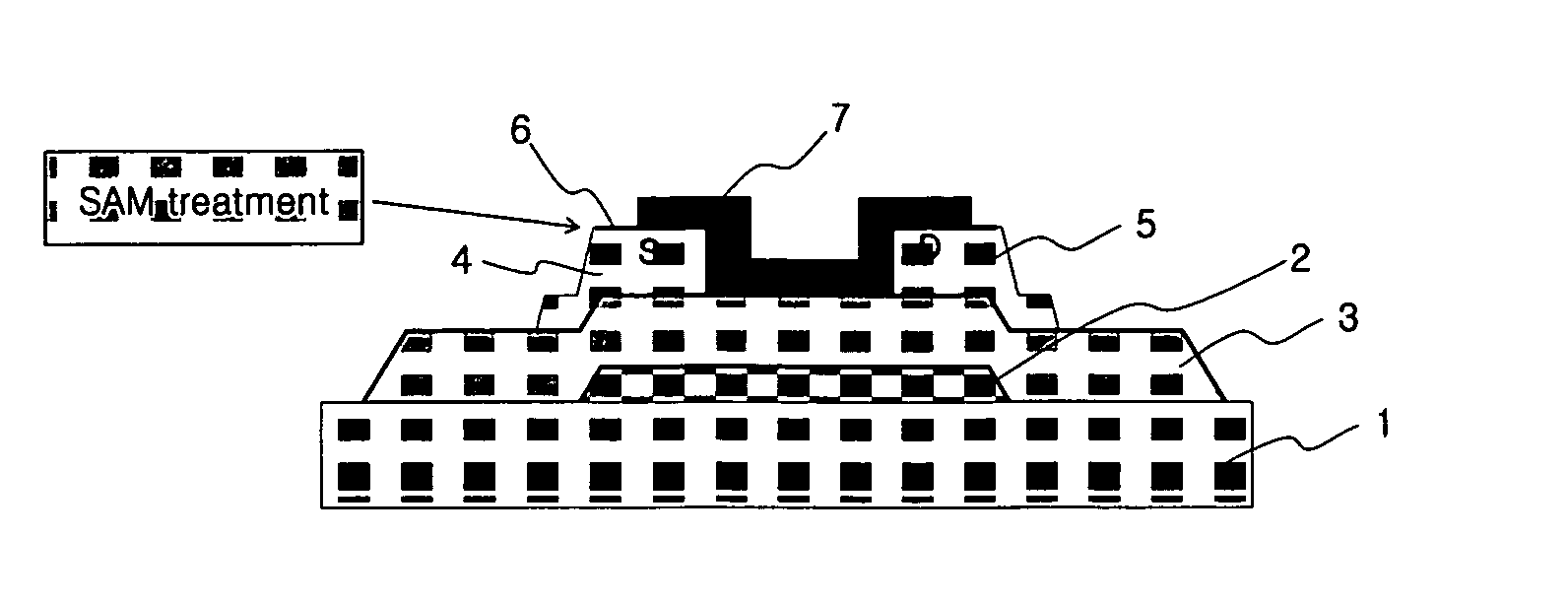
[0103] Al was deposited on a clean glass substrate by a sputtering technique to form a gate electrode having a thickness of 1,500 Å. Polyvinylphenol containing a crosslinking agent was spin-coated thereon at 1,000 rpm to a thickness of 5,000 Å, and soft-baked at 100° C. for 5 minutes to form a gate insulating layer. ITO was deposited on the insulating layer to a thickness of 1,000 Å by a thermal evaporation method, and was then subjected to photolithography to form an ITO electrode pattern. At this time, the deposition was conducted under a vacuum pressure of 2×10⁻⁷ torr, a substrate temperature of 50° C. and at a deposition rate of 0.85 Å / sec. Subsequently, the ITO electrode was surface-treated by impregnating it with a self-assembled monolayer forming solution at room temperature for 30 minutes. The self-assembled monolayer forming solution was prepared by dissolving 5 wt % (based on a total weight of the solution) of a perfluorinated resin solution (Nafion®, Aldrich) in a mixed s...

example 2

[0106] An organic thin film transistor was fabricated in the same manner as in Example 1, except that the surface of the ITO electrode was acid-treated with an ITO etchant (HCl—16.7-20.3% in water) at room temperature for 10 seconds.

example 3

[0107] An organic thin film transistor was fabricated in the same manner as in Example 1, except that the surface of the ITO electrode was subjected to UV ozonation using a lamp having a power of 0.28 W / cm3 at a wavelength of 254 nm for 3 minutes, prior to the surface treatment of the ITO electrode.


PUM


Abstract

Example embodiments of the present invention for fabricating an organic thin film transistor including a substrate, a gate electrode, a gate insulating layer, metal oxide source/drain electrodes and an organic semiconductor layer wherein the metal oxide source/drain electrodes are surface-treated with a self-assembled monolayer (SAM) forming compound containing a sulfonic acid group. According to example embodiments of the present invention, the surface of the source/drain electrodes may be modified to be more hydrophobic and/or the work function of a metal oxide constituting the source/drain electrodes may be increased to above that of an organic semiconductor material constituting the organic semiconductor layer. Organic thin film transistors fabricated according to one or more example embodiments of the present invention may exhibit higher charge carrier mobility. Also disclosed are various example devices including display devices having organic thin film transistors made by example embodiments of the present invention.

Description

PRIORITY STATEMENT [0001] This non-provisional application claims priority under 35 U.S.C. § 119 of Korean Patent Application No. 2005-56196 filed on Jun. 28, 2005, the entire contents of which are incorporated herein by reference. BACKGROUND OF THE INVENTION [0002] 1. Field of the Invention [0003] Example embodiments of the present invention relate to an organic thin film transistor and to a method for fabricating the same. More particularly, example embodiments of the present invention relate to a method for fabricating an organic thin film transistor with improved (e.g., higher) charge carrier mobility. According to example embodiments of the present invention, the organic thin film transistor may include a substrate, a gate electrode, a gate insulating film, metal oxide source / drain electrodes and an organic semiconductor layer. In example embodiments of the present invention, the metal oxide source / drain electrodes may be surface-treated with a self-assembled monolayer (SAM) fo...

Claims


Application Information

Patent Timeline
IPC IPC(8): H01L51/00H01L51/40
CPCH01L51/0055H01L51/105H01L51/052H10K85/623H10K10/471H10K10/84
Inventor PARK, HYUN JUNGLEE, SANG YOONJEONG, EUN JEONGHAN, KOOK MINHAHN, JUNG SEOKLEE, TAE WOO
Owner SAMSUNG ELECTRONICS CO LTD
Why Eureka
Try Eureka